Download
1 / 50
520 likes | 590 Views
DMT 234 LECTURE 6 P-N JUNCTION. NOR ROSHIDAH YUSOF SCHOOL OF MICROELECTRONIC ENGINEERING. PART I pn junction at zero bias. SUBTOPIC. BASIC STRUCTURE OF THE PN JUNCTION PN JUNCTION CHARACTERISTIC UNDER ZERO APPLIED BIAS :- BUILT-IN POTENTIAL ELECTRIC FIELD SPACE CHARGED WIDTH.

E N D
DMT 234 LECTURE 6P-N JUNCTION NOR ROSHIDAH YUSOF SCHOOL OF MICROELECTRONIC ENGINEERING
SUBTOPIC • BASIC STRUCTURE OF THE PN JUNCTION • PN JUNCTION CHARACTERISTIC UNDER ZERO APPLIED BIAS :- • BUILT-IN POTENTIAL • ELECTRIC FIELD • SPACE CHARGED WIDTH
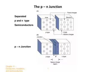
BASIC STRUCTURE OF pn JUNCTION n -TYPE p -TYPE Majority : hole ( mobile) Minority : negative acceptor ion ( fixed) Majority : electron( mobile) Minority : positive donor ion ( fixed)
BASIC STRUCTURE OF pn JUNCTION EC EFi EF EC EV EF EFi EV
BASIC STRUCTURE OF pn JUNCTION • p and n semiconductor are brought closer • electron (n-region) will diffuse to p-region & left the positively charged donor atom • hole (p-region) will diffuse to n-region & left the negatively charge acceptor atom • positive and negative charge in metallurgical junction will induce electric field from n- to p-region ( + - )
BASIC STRUCTURE OF pn JUNCTION Fig. (a) : Uniformly doped p-type and n-type semiconductor before the junction is formed Fig. (b) : Electric field in the depletion region and energy band diagram of a p-n junction in thermal equilibrium
The net positively and negatively charged regions are shown in figure below. • These two regions are referred as the space charge or depletion region. • All electrons and holes are swept out of the space charge region by the electric field. • Diffusion force act on the electrons and holes at the edges of the space region. • The electric field in space charge produces another force on the electron and holes which is in the opposite direction to the diffusion force for each type of particle. • In equilibrium, the diffusion force and E-field force exactly balance each other.
ZERO APPLIED BIAS • Examine the properties of the step junction in thermal equilibrium, where no currents exist and no external excitation in applied. • Determine the space region width, electric field and potential through the depletion region.
BUILT-IN POTENTIAL BARRIER • Assume no voltage is applied across pn junction (thermal equilibrium condition) • The Fermi energy level will be constant • Conduction and valance band energies are BEND as we go through the space charge region. • Electron in Ec of the n region see a potential barrier in trying to move into the Ec of the p region. • This potential barrier referred to as the built-in potential barrier and is denoted by Vbi. • Vbi maintains equilibrium if no current is produced by this voltage.
EXAMPLE Calculate the built-in potential for a silicon p-n junction with Na= 2 x 1017 cm-3 and Nd = 1015 cm-3 at 300K. Assume that ni = 1.5 x 1010 cm-3. Answer: 0.713 V
EXERCISE • Calculate the built-in potential barrier in a GaAs p-n junction at T = 300 K for • Na= 5 x 1015 cm-3 and Nd = 1017 cm-3 • Na= 2 x 1016 cm-3 and Nd = 2 x 1015 cm-3 • Assume that ni = 1.8 x 106 cm-3.
ELECTRIC FIELD • Electric field is created in the depletion region by the separation of positive and negative space charge densities. • The space charge region abruptly ends in the n region at x = +xnand abruptly ends in the p region at x = -xp
Electric field in p-region Electric field in n-region The number of negative charges per unit area in the p-region is EQUAL to the number of positive charges per unit area in the n-region
POTENTIAL • Potential is determine by integrating the electric field Therefore, Note : The magnitude of the potential at x = xnis equal to the built-in potential barrier.
SPACE CHARGE WIDTH The distance that the space charge region extends into the p and n regions from the metallurgical junction. solve The total depletion or space charge width, W
exercise Consider a silicon pn junction at T = 300K with doping concentrations of Na = 2 x 1017 cm-3 and Nd = 1015 cm-3. Calculate • Built in potential barrier, Vbi • Space charge width, W • Electric field, E • in pn junction with zero bias.
SUBTOPIC • IN THIS CHAPTER WE WILL CONSIDER THE PN JUNCTION IN FORWARD BIAS, REVERSE BIAS AND BREAKDOWN. • PN JUNCTION DIODE ITSELF PROVIDES CHARACTERISTICS THAT ARE USED IN RECTIFIERS AND SWITCHING CIRCUIT.
INTRODUCTION • When voltage (reverse / forward bias) is apply to pn junction, the system is no longer in equilibrium condition as the following parameter will be changed:- • Built-in potential • Electric Field • Space Charge Width
ZERO BIAS FORWARD BIAS REVERSE BIAS • Positive voltage is applied to n-region with respect to p-region • Vtotal = Vbi+ VR • Space charge region is wider • Under equilibrium at zero voltage • Positive voltage is applied to p-region with respect to n-region • Vtotal = Vbi - Va • Space charge region is thicker
ZERO BIAS FORWARD BIAS REVERSE BIAS • Fermi energy for the n region is lower than that in the p region. • The total potential barrier is larger. • The increased in the potential barrier continues to hold back the electrons and holes so that there is still essentially no charge flow and hence no current. • The potential barrier seen by the electrons holds back the large concentration of electrons in the n region and keeps them from flowing into the p region. Similarly goes for the holes. Pn junction in thermal equilibrium. • The Fermi level in the p region is lower than that in the n region. • The total potential barrier is now reduced the E field in the depletion region is also reduced. • The diffusion of holes and electrons across the space charge region will occur and generates a current through the pn junction
FORWARD BIAS CONDITION • The potential barrier of pn junction is lowered when forward bias voltage is applied, allow electrons and holes to flow across the space charge region. • When holes from p region across the space charge region to n region it will become excess minority carrier holes. Eelctron also will become excess minority carrier electrons in p region. • When a forward bias apply, a small sinusoidal voltage superimposed on dc voltage applied across a pn junction will generate a small-signal sinusoidal current. • The ratio of sinusoidal current to voltage yields the small-signal admittance of the pn junction. • The admitance of forward bias pn junctions contains both conductance and capacitance called as a diffusion capacitance.
IDEAL CURRENT-VOLTAGE RELATIONSHIP • Four assumptions for the ideal I-V derivation: • The abrupt depletion layer approximation applies. The space charge regions have abrupt boundaries and the s/c is neutral outside of the depletion region. • 2. The Maxwell-Boltzmann approximation applies to carrier statistics • The concept of low injection applies • a. The total current is constant throughout the entire pn structure • b. The individual electron and hole currents are continuous functions through the pn structure • c. The individual electron and hole currents are constant throughout the depletion region
DMT 234 Semiconductor Physic & Device Mnorhafiz 2011
FORWARD BIAS Apply forward voltage means: + applied to P-side and - applied to N-side Effect is opposite of that described above: (i) Vforward subtracts for built-in barrier Vbi (ii) Enhances chance of additional carriers crossing junction (iii) Possibility of steady-state current flow
REVERSE BIAS • Apply reverse voltage means: + applied to N-side and - applied to P-side • Remember that Voltage = potential energy per positive charge • Positive voltage pulls DOWN electron energy !! Fermi levels no longer match on both sides: EFp > EFn ; EFp – EFn = e.Vreverse
Reverse bias sucks carrier out of bar: Expose more Na- and Nd+ Increase dipole E field Increase voltage step across junction
New equations that include finite applied reverse bias Only change: substituted ( Vbi + Vreverse ), the new total barrier, for old Vbi
DMT 234 Semiconductor Physic & Device 6.6 Junction capacitance Basically, the junction depletion layer capacitance/area is defined as Cj=dQ/dV, where dQ – incremental change in depletion layer/unit area for an incremental change in the applied voltage dV. Differential change in the space charge width with a differential charge in reverse-bias voltage for a uniformly doped pn junction.
DMT 234 Semiconductor Physic & Device 6.7 One sided junction One-sided junctions - one side of the pn junction is much more heavily doped than the adjacent side)
BOUNDARY CONDITION If assume complete ionization This equation relates the minority carrier electron concentration on the p side of the junction to the majority carrier electron concentration on the n side of the junction in thermal equilibrium.
DMT 234 Semiconductor Physic & Device If a bias is supplied to the pn junction diode, then: Fig. : (a) A pn junction with an applied forward-bias voltage showing the directions of the electric field induced by Va and the space charge electric field. (b) Energy band diagram of the forward-biased pn junction
Boundary condition at the space charge edge Similarly, the holes relationship is also written as: Boundary condition at the space charge edge Fig. : Excess minority carrier concentrations at the space charge edges by the forward-bias voltage.
Minority Carrier Distribution: The ambipolar transport equation in the n-region:
In the n-region for x > xn, we have that E=0 and g’=0. Also assume steady state so Similarly in the p-region:
The general solution for the n-region & p-region Using the boundary conditions We can obtain the excess carrier conc.
Ideal pn junction current Fig. :Steady-state minority carrier concentrations in a pn junction under forward bias The minority carrier diffusion currents:
The total current density in the pn junction is then: where Js – saturation current density and is defined as: Notes: Since we are assuming the electric field is zero at the space charge edges, we can neglect any minority carrier drift current component.
Fig. : Ideal IV characteristics of a pn junction diode with the current plotted on a log scale Fig. : Ideal IV characteristics of a pn junction diode
Exercise 1: A silicon pn junction at T=300K with zero applied bias has doping concentrations of Nd= 5 x 1016 cm-3 and Na= 5 x 1015 cm-3. Determine xn, xp, W and |Emax| [Answer: xn= 4.11 x 10⁻⁶ cm, xp=4.11 x 10⁻⁵ cm, W= 4.52 x 10⁻⁵ cm, |Emax|=3.18 x 10⁴ V/cm]
Exercise 2: A silicon pn junction at T=300K is reverse biased at VR=8V. The doping concentrations are Na= 5 x 1016 cm-3 and Nd= 5 x 1015 cm-3. Determine xn, xp, W and |Emax| [Answer: xn= 1.43 x 10⁻⁴ cm, xp=1.43 x 10⁻⁵ cm, W= 1.57 x 10⁻⁴ cm, |Emax|=1.11 x 10⁵ V/cm]
Next Topic : Metal semiconductor, semiconductor haterojunctions & Bipolar Transistor.