Download
1 / 29
310 likes | 814 Views
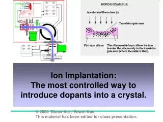
Ion Implantation: The most controlled way to introduce dopants into a crystal. Image of the Day. What could this be ????. www.appliedmaterials.com. And it is …. A Swift Implanter. www.appliedmaterials.com.

E N D
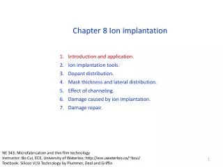
Ion Implantation:The most controlled way to introduce dopants into a crystal.
Image of the Day What could this be ???? www.appliedmaterials.com
And it is …. A Swift Implanter www.appliedmaterials.com Current implant products include the xR80S, which performs implants in the energy range of 2 to 80keV; the xR120S for energy ranges of 2 to 120 keV; and the xR LEAP for energy ranges of 200eV to 80keV. All these products provide a significant increase in productivity and a dramatic decrease in footprint size over traditional implant systems. The xR200S, an updated version of the Precision Implant 9500xR, operates over an energy range of 2 to 200keV, with an option to perform phosphorous implants up to 720keV.
Ion Implantation • Introducing dopants by diffusion had three major drawbacks: • Surface concentration and depth were coupled. • Essentially, only Gaussian and erfc profiles could be generated. • The process was not precisely reproducible - an effect which we now know reflects various concentration of point defects (vacancies, interestitials etc). • Ion implantation fixes these problems at the cost of crystal damage. • Variable profiles, precise control over amount of impurities. For a history, as well as a general excellent WEB reference click here: http://courses.nus.edu.sg/course/phyweets/Projects98/proj3204/ion_mpage.htm
A typical implanter has an ion source accelerator filtering magnet deflection/scanning coils or plates incident current meter Typical voltages are 50 to 200 KeV, the trend is to lower voltages.
To make the ions, a neutral gas, such as BF2 is introduced into the ion source and turned into ions by bombarding it with electrons (the black loop). The source is at a very high positive potential respective to ground (hundreds of kilovolts). Getting the gas, stored at a bottle at ground potential, up into the source without a “Short” is not trivial. Neither is control and powering of the electron emitting filament.
The ions are accelerated in steps by letting them “fall down” in e.g. 50 KeV steps from + 200 Kev (relative to ground) to ground. It can’t be done in one step, as you would likely get arcing
The ions are filtered by sending them trough a magnetic field F = q (v x B) Lighter ions move faster and experience higher radial forces. Heavier ions lower ones. This sorts out impurities as well as BF2++ (double charged ions)
The filtered ion beam is expanded (electrostatic lens) and scanned over the wafer. Some accelerators scan by moving the substrate, others be deflecting the beam, and yet others use a combination (e.g. deflection for x and mechanical movement for y) The incident current is measured as it is a very accurate measurement of the dose
How the ions lose energy in the solid (Ion stopping) Their final distribution in the solid (Range, straggle) The damage they do to the crystal (EOR damage) How to anneal out the damage (Dopant activation) What do we need to know…
Ion Implantation Ion Stopping Channeling Damage Equipment Annealing Outline
Incident Ion Energies Stopping Power Nuclear Electronic Ion Stopping
B -> Si Stop Profiles B Implant a-Si Target No Annealing SIMS Data Stop Profiles - Gaussian - Pearson IV
2D Implant Profile Example Note how “dopant crawls under mask” Implant P, 150 keV Rp = 190 nm DRp = 63 nm 2 mm Window 3.2 x 0.6 mm Si D = 0.8x10⁻¹⁵ cm2/s After Krusius et al, IEEE TED-29, p. 435 (1982) The “sideways” extension is sometimes characterized by yet an other parameter: “lateral straggle”
2D Implant Profile Example Since the implant must be annealed to activate the dopants, there is further movement. The D for this step is not the D in the tables… it is enhanced by point defects introduced by the implantation (“transient enhanced diffusion”, excellently treated in Plummer) Implant + Diffusion P, 150 keV Rp = 190 nm DRp = 63 nm 2 mm Window 3.2 x 0.6 mm Si D = 0.8x10⁻¹⁵ cm2/s Krusius et al, IEEE TED-29, p. 435 (1982)
2D Implant Profile Example Here is what happens if the “Dt” product is larger than expected ! Implant + Diffusion P, 150 keV Rp = 190 nm DRp = 63 nm 2 mm Window 3.2 x 0.6 mm Si D = 0.8x10⁻¹⁵ cm2/s Krusius et al, IEEE TED-29, p. 435 (1982)
Si Crystal Faces (100) Tilted (100) (111) Ion Channeling
In certain crystallographic directions, noticeably [110], ions travel much deeper into the crystal than expected. The effect, explained next, is caused by “open channels” in the crystal structure. The effect is a nuisance in the IC industry. To turn it off, wafers are deliberately tilted such that the beam sees no open channels Ion channeling
Channeling Concept Ion Ion Scattered into Channel Recoil Channeled Ion Target Atom Row Si Channel
Si Crystal Faces After Runyan & Bean, Fig. 9-15 (100) Si Face 7o Tilt, 30o Twist (100) Si Face
Target Atom Recoils Absorption of Energy Generation of Vacancies Point Defect and Ion Distributions Critical Dose for Amorphization Ion Damage
The incident ions have very high energy. Typically e.g. 100 keV. It only takes about 20 eV to knock a silicon atom off it’s lattice site and shoot as an interstitial somewhere into the lattice. Thus, a 100 KeV atom can dislodge, very roughly, on the order of 5000 Si atom. If each dopant atom eventually lands on a lattice site, then there must be as many Si self interstitials as there are dopant atoms (e.g. 1e20/cm3). These interstitials cluster into {311} defects and end of range EOR loops Damage to Crystal lattice
Critical Dose for Amorphization Implant -> Si Continuous Amorphous Layer Critical Dose (cm-2) 11B 31P 122Sb 1000/T (K-1) Sze, Fig. 12, p. 343
Implant Damage Annealing • Function Defect Removal, Activation of Dopants • Furnace, Rapid Thermal Annealing, and Laser Annealing • Solid State Epitaxial Regrowth
Implant Annealing/Activation Ion Individual Collision Cascades for < 1012 cm-2 X-tal Surface Amorphous Layer for > 1015 cm-2 Damaged X-tal or Amorphous Annealing - SSER > 450 C - Point Defects - Extended Defects Activation - Substitutional Sites Target Atom X-tal Bulk
Annealing/Activation End-of-Range (EOR) Dislocation Loops After Solid Phase Epitaxial Regrowth Concentration PDG 8-25 2000 Depth
Activated Fraction Implant B-> Si 70 keV 1015 cm-2 Anneal 800 or 900 C 35 min 800 C 900 C Depth (mm) SIMS SIMS Hall Hall After Sze, Fig. 24, p. 357 Concentration (cm-3)
Implant/Anneal Examples 1021 Implant B-> Si 35 keV Anneals RTA 1100 C/10 s RTA 1100 C/30 s F 1000 C/30 m Concentration (cm-3) F RTA I Sze, Fig. 29, p. 362 1015 0 1 Depth (mm)
Implant/Anneal Examples Transient Enhanced Diffusion (TED) Anomalous Diffusion After Ion Implantation Concentration (cm-3) PDG 8-31 2000 Depth (mm)