SSD Science Specification Table
410 likes | 613 Views
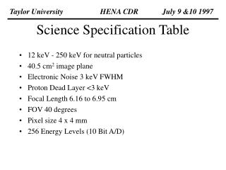
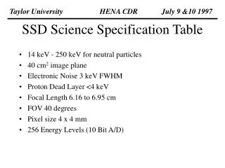
Taylor University HENA CDR July 9 &10 1997. SSD Science Specification Table. 14 keV - 250 keV for neutral particles 40 cm 2 image plane Electronic Noise 3 keV FWHM Proton Dead Layer <4 keV Focal Length 6.16 to 6.95 cm FOV 40 degrees Pixel size 4 x 4 mm

SSD Science Specification Table
E N D
Presentation Transcript
Taylor University HENA CDR July 9 &10 1997 SSD Science Specification Table • 14 keV - 250 keV for neutral particles • 40 cm2 image plane • Electronic Noise 3 keV FWHM • Proton Dead Layer <4 keV • Focal Length 6.16 to 6.95 cm • FOV 40 degrees • Pixel size 4 x 4 mm • 256 Energy Levels (10 Bit A/D)
Taylor University HENA CDR July 9 & 10 1997 Engineering Specification Table • Sensors: XY Position Si solid state sensors • Two vendors used: Canberra and Micron • Analog Electronics 240 A225 preamplifiers 15 ASIC amplifiers • Total Power 3 Watts (at supply voltages) • Voltages +/- 5 analog, +5 dig., and bias voltage (-70V) • Planned Temperature Operation 0o C +- 20o C • Survival Temperature: +60oC to -50oC
Taylor University HENA CDR July 9 & 10 1997 SENSOR SPECIFICATIONS • MEASURES NEUTRALS E>14 keV • 4 - 60 ELEMENT ARRAY (12 X 5) • ACTIVE AREA: 48.7mm x 20.8mm per SSD • THICKNESS: >200 MICRONS • THIN WINDOW: <5 keV H+ ENERGY LOSS (Si) • BIAS APPLIED TO THIN WINDOW SIDE OPPOSITE PIXELS • LEAKAGE CURENT: <10nA • ELECTRONIC NOISE RESOLUTION: <1KeV FWHM • BOND PADS: 4 - 5 MILS • BOND WIRES: < 1.25 MILS
Taylor University HENA CDR July 9 & 10 1997 SSD Design Features • Parallel processing (240 channels) • High resolution (240 pixel array @ 256 Energy levels) • Adjustable Thresholds and Control Logic • Low Power • Single Box Assembly
Taylor University HENA CDR July 9 & 10 1997 Design Philosophy • Use Existing Technology • Use Well Proven Analog Gate Array Technology • High reliability, Parallel Processing, Low Power, and Low Complexity • Rigorous Testing and Burn-In of Subsystems • State-of-the-Art Instrument
Taylor University HENA CDR July 9 & 10 1997 System Design
Taylor University HENA CDR July 9 & 10 1997 SSD Detector Holder Rendering Metalized PC Card SSD Shields Platform
Taylor University HENA CDR July 9 & 10 1997 SSD Mounting Assembly
Taylor University HENA CDR July 9 & 10 1997 SSD Detector Assembly
Taylor University HENA CDR July 9 & 10 1997 Shield Holder
Taylor University HENA CDR July 9 & 10 1997 PC Board Shield
Taylor University HENA CDR July 9 & 10 1997 Preamplifier Board Rendering Flex Cable Connection 60 A225 Preamps 4 FEA Chips Actel Chip MDM Connector
Taylor University HENA CDR July 9 & 10 1997 A225 Preamplifier Repackaging A225 will be repackaged in A111F casing
Taylor University HENA CDR July 9 & 10 1997 HENA Middle Box Design
Taylor University HENA CDR July 9 & 10 1997 SSD Cap., Noise, Thickness
Taylor University HENA CDR July 9 & 10 1997 Pixel Angular Resolution from Center of Pin Hole
Taylor University HENA CDR July 9 & 10 1997 Ion Penetration in Silicon Standard Window N+ Side Enhanced Window N+ side Standard Window P+ junction Enhanced Window P+ junction
Taylor University HENA CDR July 9 & 10 1997 Detector Geometry
Taylor University HENA CDR July 9 & 10 1997 Sensor Mount Finite Element Model PC Board Frame Sensor #2 Mount C L Nodes: 576 Size: 2.49E-2 x 10.21E-2 m Thickness: 12.7E-4 m Sensor #1 Mount
Taylor University HENA CDR July 9 & 10 1997 Vendor Response List Name of Vendor Status • Canberra Completed Design and Mask, In Fabrication, On Schedule • Micron Completed Design, Mask started ~4 Weeks behind schedule
Taylor University HENA CDR July 9 & 10 1997 FEA Microcircuit Heritage POLAR Satellite • FEA Micro circuits • POLAR Satellite • SEPS • IPS • PIXIE (Polar Ionospheric X-Ray Imaging Experiment) • SPADUS (flew on the Argos satellite) • MAXIE (Magnetospheric Atmosphere X-Ray Imaging Experiment) flew on Aug. 9, 1993 on the TIROS satellite. It measured x-rays in the range of 4 - 100 keV. SEPS SPADUS
Taylor University HENA CDR July 9 & 10 1997 IMAGE Front-end Gate Array Features • 16 amps - each has a calibration pulser input, low gain (proton mode) and high gain (electron mode) sections, and test outputs via a diagnostic MUX for each gain. • 17 peak holding circuits -- 16 XY pixels and on E detector pixel. • 16 electron mode comparators with individually adjustable thresholds • 16 proton mode comparators with a common adjustable reference • Micro computer data input to configure the chip. • Logic disable gates for each pixel and each anti. • Set-up latches (113 bits) to configure the chip • Mode control latches. • Coincidence logic with adjustable resolving time. • Programmable anti coincidence logic including pile-up rejection • Tri-state outputs controlled by a polling clock.
Taylor University HENA CDR July 9 & 10 1997 PHA/ Scaler Gate Array Features • 16-channel stacked discriminator (log/linear) with programmable endpoints set by two 8-bit DACs • Eight 16-bit scalers with overflow bits and buffers • 16-bit computer bus interface • Set-up latches (24 bits) • State logic directs the collection and storage of spectra in a dedicated 8K x 8 RAM • The RAM is organized as 4K 16-bit words • Data router and increment logic accumulate up to 256 16-channel spectra • Control logic to multiplex four front-end chips and isolate them from the computer bus • 3-to-8 decoder with five external outputs
Taylor University HENA CDR July 9 & 10 1997 Block Diagram of PHA chip
Taylor University HENA CDR July 9 & 10 1997 I/O Gate Array Features • 16-bit computer interface with 4-bit address decode • Control registers (44 bits) • Serial input/output with an 8-bit buffer • Eight-bit counter/timer with an adjustable pre-divide • Watch-dog timer for resetting microprocessor • Digital-to-analog converter with a pulser mode • Analog-to-digital converter with an eight-input MUX • Dual eight-bit bi-directional parallel ports • Vectored interrupt logic (five internal). The three external interupts may be edge or level triggered. • Status register • Crystal oscillator (generates computer clock) • Power-on reset circuit
Taylor University HENA CDR July 9 & 10 1997 I/O Chip Block Diagram
Taylor University HENA CDR July 9 & 10 1997 A225 Characteristics • Operation Temp: -55oC to + 125oC • Operation Voltage: +4 to +25 VDC • Sensitivity: 240 mv/Mev (Si) • Noise: 2.4 Kev FWHM (Si) • Noise Slope: 50 ev/pf (Si) • Radiation Resistance: 105 Rads Input: 5 mV, 2ms Output: 175mV, 6ms
Taylor University HENA CDR July 9 & 10 1997 ASIC’s Amplifier Chain Schematic
Taylor University HENA CDR July 9 & 10 1997 Main Electrical SSD Components
Taylor University HENA CDR July 9 & 10 1997 Interface Signals
Taylor University HENA CDR July 9 & 10 1997 Memory MAP
Taylor University HENA CDR July 9 & 10 1997 PHA Register Map
Taylor University HENA CDR July 9 & 10 1997 Front-End Register Map
Taylor University HENA CDR July 9 & 10 1997 IO Chip Register Map
Taylor University HENA CDR July 9 & 10 1997 Actel Chip Signals ACIEL ACT1 FPGA signals: AD[0..7] 8-bit bi-directionaladdress/data bus Inputs: Win[0..14] Event windows, one from each FEA Anti Event anti--on tri-state bus--poll FEA to activate POR Power-on reset--from I/O gate array CS* Chip select--from PHA decoder ALE Address latch enable--from DPU WR* Write strobe--from DPU RD* Read strobe--from DPU (may not need) DPU[0..7] Time-of-flight data--from DPU CLK 3.2 MHz clock--from I/O gate array Poll[0..14] Poll strobes--one to each FEA Pixel[0..7] Pixel/FEA ID register--to DPU and PHA CDPU[0..2] Compressed time-of-flight data--to RAM address bits A[13..15] RST Reset--to FEA gate arrays; only polled FEA will reset Start Starts PHA cycle Etrig Event trigger--to DPU Outputs:
Taylor University HENA CDR July 9 & 10 1997 FE Chip Signals
Taylor University HENA CDR July 9 & 10 1997 PHA Signals