Low-Power SRAM ECE 4332 Fall 2010
170 likes | 328 Views
Low-Power SRAM ECE 4332 Fall 2010. Team 2: Yanran Chen Cary Converse Chenqian Gan David Moore. Metric. Metric = (Active Energy per Access) 2 *Delay*Area*IdlePower Active Energy per Access = 9.704 fJ Delay = 7.186 ns Area = ~1.2 mm 2 Idle Power = 57.78 uW

Low-Power SRAM ECE 4332 Fall 2010
E N D
Presentation Transcript
Low-Power SRAMECE 4332 Fall 2010 Team 2: Yanran Chen Cary Converse Chenqian Gan David Moore
Metric Metric = (Active Energy per Access)2*Delay*Area*IdlePower • Active Energy per Access = 9.704 fJ • Delay = 7.186 ns • Area = ~1.2 mm2 • Idle Power = 57.78 uW • Our Metric = 4.692e-41 J2*s*mm2*W
Metric Breakdown Values • 1 Bitcell Area = 0.649 um2 • Read Energy = 9.678 fJ • Write Energy = 9.834 fJ • Read Delay = 7.186 ns • Write Delay = 6.491 ns • Idle Power = 57.71 uW • With 0.3 V VDDsleep => 0.483 uW
Special Features Overview • Latching Voltage Sense Amplifier • Low Voltage (w/ sleep mode) • Single Bit Error Correcting Code
Latching Voltage Sense Amplifier • Minimizes BL sagging to reduce the energy/read • Allows faster read Modified from Ryan & Calhoun, 2008
Low Voltage Sleep VDD 0.35v 0.30v 0.25v Data Retention Voltage: • 0.6 V for active operation • 0.3 V for sleep mode HOLD butterfly plots at lower voltages indicate data can be retained when sleep voltage is as low as 0.3 V.
Single Bit Error Correcting Code • Importance: • Compensate for smaller SNMs due to lower voltage • Maintaining important data • Hamming Code: • 6 Parity Bits • 32 Data Bits • Allows correction of 1 error per word, detection of 2 errors per word • Process: • Determine parity bits at Write • Correct word at Read
Single Bit ECC, continued • Requires significant overhead: • Area • Delay • Power • Additional components required: • Parity generation/check circuits: XORs • Decoder • Correction circuit: Inverter, 2:1 Multiplexer
ECC Diagram Parity Bit Generation (at write) Parity Checking & Correction (at read)
Design Considerations • Ensure Voltage is high enough to protect data • Avoid extreme delay due to low voltage • Minimize impact of ECC on area, delay • Memory block division
Block Size • Tradeoff between block complexity and top level complexity • Smaller blocks have lower access energy as shown using data from an early model • Additional blocks require wider output muxes, more complicated distribution of Input Data • Chose to use 16 256x256 blocks - later extended for ECC
Layout/ Notes on topology • High Vt bitcells to reduce leakage, and require less cell ratio, pull down ratio reduced area • Blocks of memory to decrease WL capacitance
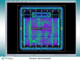
Block Layout (64kb) • All Row Periphery, Column Periphery Complete • Array consumes majority of area • Uses metal4 and lower
Sources • ECE 4332 2009 Group Projects Pages. UVa ECE Wiki. • Kaxiras, S., Zhigang, H., & Martonosi, M. Cache Decay: Exploiting Generational Behavior to Reduce Cache Leakage Power. 9th International Symposium on Computer Architecture, 2001. • Ling, S., Kim, Y. B., & Lombardi, F. A Low-Leakage 9T SRAM Cell for Ultra-Low Power Operation, 2008. • Rabaey, J. Digital Integrated Circuits: A Design Perspective. Prentice Hall, 2003. • Ryan, J. F., & Calhoun, B. H. Minimizing Offset for Latching Voltage Mode Sense Amplifiers for Sub-Threshold Operation. 9th International Symposium on Quality Electronic Design, 2008. • Wang, A., Calhoun, B. H., & Chandrakasan, A. P. Sub-Threshold Design for Ultra Low-Power Systems. Springer, 2006.
