Download
1 / 56
830 likes | 1.93k Views
Introduction to Analog-to-Digital Converters. Shraga Kraus. ADC. Contents. Time-Interleaved Structure Characterization in the Lab Discussion. Background Some Basic Analog Circuits ADC Architectures Flash ADC Folding ADC Algorithmic ADCs Pipeline ADC. Background. ADC Model (1/2).

E N D
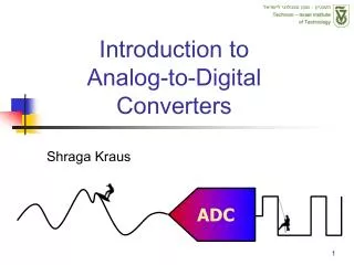
Introduction to Analog-to-Digital Converters Shraga Kraus ADC
Contents • Time-Interleaved Structure • Characterization in the Lab • Discussion • Background • Some Basic Analog Circuits • ADC Architectures • Flash ADC • Folding ADC • Algorithmic ADCs • Pipeline ADC
ADC Model (1/2) • Analog signal: continuous both in time and value • Digital signal: discrete both in time and value • Discrete time (sampling) aliasing • Discrete value (resolution) quantization
ADC Model (2/2) • Modeled as a linear system + quantization noise • For easy analog treatment, noise is input-referred noise
Sampling for Dummies (1/3) • Sampling = multiplication by an impulse train • Y(t) = X(t) · S(t) • Ts = sampling interval • fs = 1/Ts = sampling frequency Ts t
Sampling for Dummies (2/3) • In the frequency domain: • Y(f) = X(f) *S(f) • “Aliasing” is evident
Sampling for Dummies (3/3) • Nyquist sampling: • Over-sampling: • Under-sampling:
Anti-Aliasing Filter • Nyquist sampling: • Over-sampling: • Under-sampling:
Incoherence – by Comics • Consider the following sinusoidal inputs, sampled at fs: t
Quantization (1/4) • Δ = LSB • m = num of bits • Full scale amplitude: 7 6 5 4 3 2 1 0 A 0 Δ
Quantization (2/4) • For incoherent sinusoidal input: • Assuming uniform distribution of quantization noise from –Δ/2 to +Δ/2 Fqn 1/Δ x –Δ/2 0 +Δ/2
Quantization (3/4) • For incoherent sinusoidal input with full scale amplitude: • Signal power: • Noise power:
Quantization (4/4) • SNR: • Effective number of bits (ENOB):
Example • Simulated ideal 7-bit ADC: • SNR = 43.8 dB ENOB = 7
Practical Over-Sampling • Out-of-band noise is filtered out digitally • OSR = 2 SNR x2 (+3dB) ENOB +½
Non-Linear Effects (1/2) • Integral Non-Linearity (INL) output code 7 6 5 4 3 2 1 0 Vin 0 Vref
Non-Linear Effects (2/2) • Differential Non-Linearity (DNL) output code 7 6 5 4 3 2 1 0 Vin 0 Vref
Differential Pair • The core of every op amp • Finite gain (Av = gmRD) • Finite bandwidth • Finite slew rate • Input capacitance • Non-linearity
Voltage Buffer (1/2) • Theoretically Vout = Vin • Finite gain results in output offest • Finite bandwidth (esp. with 2 stages) • Finite settling time • Input capacitance reduced by feedback, but still exists
Voltage Buffer (2/2) • Settling time: damping Tsettling Output Voltage slew rate Time
Switch (CMOS Only!) (1/2) • Has finite resistance • Resistance depends on the input voltage (linearity issues) • Parasitic capacitances result in charge sharing • Complicated correction circuits
Switch (CMOS Only!) (2/2) • Resistance depends on the input voltage (linearity issues)
Comparator • Basically an open-loop op amp • Must make a decision quickly • Memory effect • Input capacitance not reduced by feedback • Latched comparator – triggered by clock
Sample & Hold • Triggered by clock • Finite settling time • Must be very accurate when placed at the ADC’s input (noise/linearity) • Speed and accuracy are achieved only by very complicated circuits
Implementation Methods • Discrete time • Requires switches • Takes advantage of switched capacitors • Continuous Time • 1 clock cycle / decision • Frequencies set by absolute R-C values
Flash ADC • Continuous Time • No. of comparators = 2m – 1 • Output in thermometer code • Thermometer code is converted to binary by simple logic • Fastest topology 0011111=‘101=5
Flash ADC Limitations • Many comparators – a lot of area & power • Resistors must be matched (area) • Input drives comparators’ capacitances • Number of bits is limited (~ 5 bits)
Non-Linearity of Flash ADC • Resistor ladder mismatch • Input buffer • CLK/vin skew or input S&H non-linearity • Comparators’ “memory effect”
vout VREF vin VREF Folding ADC • Continuous Time • No. of comparators = 2m/2 (approx.) • Fast with quite a high resolution • Common in instrumentation
Folding ADC Limitations • Flash drawbacks are alleviated, but still there • The folding amplifier must fold accurately and be linear • The folding amplifier introduces a delay and result in skew between the two flash ADCs
Non-Linearity of Folding ADC • Inherited flash non-linearity • Non-linearity of the folding amplifier • CLK/vin skew between the two flashes or input S&H non-linearity
Algorithmic ADCs • Discrete Time • Small No. of comparators (reduced area & power) • High resolution (up to 16 bits) • Digital circuitry, usually plenty of switches • Output data rate = fs /m or fs /2m (= slow…) • Types: single/dual slope, successive approximation register (SAR), integrating (Agilent’s patent) • Common in slow instrumentation and consumer devices (e.g. digital cameras)
Example: Single-Slope ADC S&H Start! Stop! VREF • Comparator’s output flips • Counter stops • Counter reset to 0 and starts counting • Slope triggered vin t
Single-Slope ADC Limitations • Calibrations are required: • Absolute R-C or L-C values • Non-linearity of the slope • Maximum time per decision: 2m clock cycles (sloooooooooooow) • S&H must be as accurate as the ADC • However: one slope + one counter can be used for many ADCs
Non-Linearity of Single-Slope • Non-linearity of the slope • Input S&H non-linearity • Incomplete capacitor discharge (“memory effect” of the slope)
Pipeline ADC • Discrete Time • No. of comparators = m • Switched capacitor circuitry • Common in CMOS
–VREF/2 then x2 C2 C1 x2 C0 ‘1’ ‘1’ ‘0’ Pipeline ADC – Example VREF = 1 V vin = 0.65 V Dout = ‘101
Pipeline ADC Limitations • Speed limited by switches and op amp settling time • The first comparator must be extremely accurate (1½ bit arch.) • Switches and op amps are lousy in contemporary CMOS technologies
Non-Linearity of Pipeline ADC • Input S&H non-linearity (if exists) • Amplifiers’ gain error (low gain) • Amplifiers’ gain different than x2 (feedback capacitor mismatch) • Amplifiers’ settling time • Inaccuracy in VREF /2 subtraction
The Principle • Using many slow ADCs • Each ADC samples the signal at a different phase t
τ τ τ The Structure vin ADC 1 CK ADC 2 ADC 3 ADC 4
Limitations • Many ADCs – area, power • Signal and clock distribution networks are required • Signal and clock distributed with different delays • Advanced RF techniques • Complicated calibration
Signal Generator Signal Generator Effective Number of Bits Pure Sine ADC