Download
1 / 19
190 likes | 315 Views
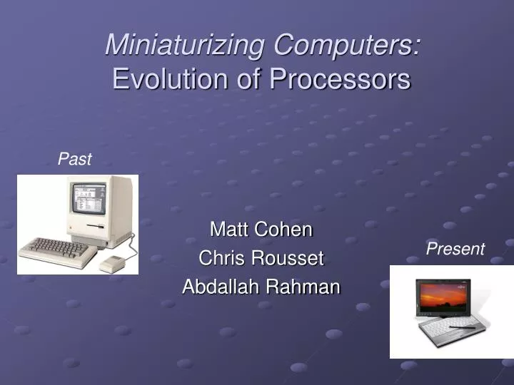
Miniaturizing Computers: Evolution of Processors. Past. Matt Cohen Chris Rousset Abdallah Rahman. Present. The Processor.

E N D
Miniaturizing Computers: Evolution of Processors Past Matt Cohen Chris Rousset Abdallah Rahman Present
The Processor A central processing unit (CPU), or sometimes simply processor, is the component in a digital computer that interprets computer program instructions and processes data. CPUs provide the fundamental digital computer trait of programmability, and are one of the necessary components found in computers of any era, along with primary storage and input/output facilities. Beginning in the mid-1970s, microprocessors of ever-increasing complexity and power gradually supplanted other designs, and today the term "CPU" is usually applied to some type of microprocessor.
The 65nm Processor The technology of today Benefits of the 90-65nm cross-over • Increase in multimedia performance (video, audio, data streaming) • Two new layers of hardware based security (protection against hackers and viruses) • Advanced manageability for IT (remote problem resolution) • Acceleration technology that improves the speed for network traffic (faster download and communication)
The 65nm Processor The 65nm technology • 35nm gate length • 1.2nm gate oxide • NiSi for low resistance • 2nd generation strained Silicon for enhanced performance These features prevent transistor leakage and reduce power consumption
The 45nm Processor Benefits of the 65-45nm cross-over • Twice improvement in transistor density • Five times reduction in source-drain leakage power • 20% improvement in transistor switching speed • 30% reduction in transistor switching power • Ten times reduction in transistor gate oxide leakage for lower power requirements and increased battery life More performance for exponentially less cost
The 45nm Processor The production • Intel is on track for 45nm production in the second half of 2007 • AMD and IBM expect the first 45nm products using immersion lithography and ultra-low-K interconnect dielectrics to be available in mid-2008
The Future • Intel plans to use extreme ultra-violet lithography to print elements as small as 32 nm and beyond (expectations 2009) • AMD and IBM will cooperate to devise techniques for manufacturing chips using the 32-nanometer and 22-nanometer processes (expectations 2009 and 2011) • Other options include replacing the use of Silicon by other materials such as Germanium • Another development relates to the use of Graphene
The Use of Germanium Why replacing Silicon? • For the past four decades the silicon industry has delivered a continuously improving performance at ever-reduced cost • Those breakthroughs were achieved by physical scaling of the silicon device • Physical limitations such as off-state leakage current and power density pose a potential threat to the performance enhancement that can obtained by geometrical scaling • Strain engineering has quickly emerged as a new scaling vector for performance enhancement to extend the life of silicon • But what will happen next?
The Use of Germanium Why using Germanium? • As seen in class mobility is one of the most important characteristics for electronic applications • According to the International Technology Roadmap for Semiconductors, even with strain engineering, metal gates and high-k dielectrics, semiconductors with higher mobility will be needed to continue scaling beyond the 22nm technology node • III/IV compounds such as InSb, InAs or InGaAs have high electron mobility but same hole mobility as Si which is an issue for p-MOS devices • Germanium is one solution
The Use of Germanium Problems with the use of Ge Germanium use will allow research and development to reach the 22nm node however: • The low bandgap (0.67eV) and low melting point (937C) poses challenges for device design and process integration • Ge wafers offer poor mechanical strength and are much more expensive than Si wafers • For n-MOS devices the presence of specific surface defects directly degrade the channel mobility and limit the current drive
The Use of Graphene • Carbon nanotubes • Metallic nanotubes display quantized ballistic conduction at room temperature • conductance can be controlled by applying an electrostatic gate • Have already been used to make simple transistors and logic gates • Low-dimensional graphite structures • Have almost identical properties of carbon nanotubes • EX: Graphene Ribbon
Nanotubes Nanotubes – many limitations - limited consistency in size and electric properties - Difficulty integrating nanotubes into electronics efficiently - High electrical resistance at junctions between nanotubes and the wires connecting them. The solution – Using Graphene layers or ribbons - Exact same properties as Carbon nanotubes with out the limitations.
Graphene layers • Advantages – • The graphene layers are only 10 atoms thick (Miniaturization) • High efficiencies and low power consumption • Devices made from graphene layers can be made using standard micro-electric processing techniques (Mass production of graphene devices) • Such standard lithographic methods
The Progress of Graphene Transistors Many universities have created transistors from graphene, approximately 80nm The goal is to make these transistors 10nm where the devices will display ballistic transport. Single-electron logic: A single-electron transistor carved entirely in a graphene sheet. The central element is a so-called quantum dot, which allows electrons to flow one by one. The dot is connected to wider regions that have contact pads used to turn the transistor on and off. Credit: University of Manchester
Problems with Graphene • Early Graphene resistors leaked current • Working on single electron transistor using quantum dots to solve this problem. • Quantum dots at room temperature are not stable enough. • No fabrication techniques available to produce the 3nm quantum dots needed for the single electron transistor. • This requires the manufacturer to once again rely on luck to produce the right sized quantum dot. This brings us back to square one as it is a similar problem with nanotubes.
Quantum Computers The future Qubits – can similtaniously be 1 and 0 at the same time, compared to bits which can only be 1 or 0. Quantum computer processes information using atoms and other tiny particles (Qubits), rather than transistors -EX: electron (Spin up down), Photon (Polarization of light horizontal, vertical) Entanglement- quantum mechanical phenomenon where the quantum states of two or more objects or qubits have to be described with reference to each other. - For example, two photons can be entangled such that if one is horizontally polarized, the other is always vertically polarized -key to quantum computers -this is what gives the quantum computer its advantage along with being simultaneously on and off. In principle a quantum computer will be able to outperform a classical computer in certain tasks
Problems of the Quantum Computer • Controlling the interaction between many qubits"The issue isn't how many qubits, it's how many well-controlled qubits," Steane says • Detecting what stat the qubits are in
Sources http://www.nature.com http://physicsweb.org/articles/news/8/6/18 http://gtresearchnews.gatech.edu/newsrelease/graphene.htm http://www.technologyreview.com/Infotech/18264/page1/ http://www.physics.gatech.edu/npeg/npeg.html http://en.wikipedia.org/wiki/Moore's_law http://www.eetimes.com/news/semi/showArticle.jhtml?articleID=196901271 http://www.amd.com/us-en/Processors/ProductInformation/0,,30_118_9485_13041%5E14633,00.html http://www.intel.com/technology/silicon/65nm-cross-over.htm