Download
1 / 24
260 likes | 438 Views
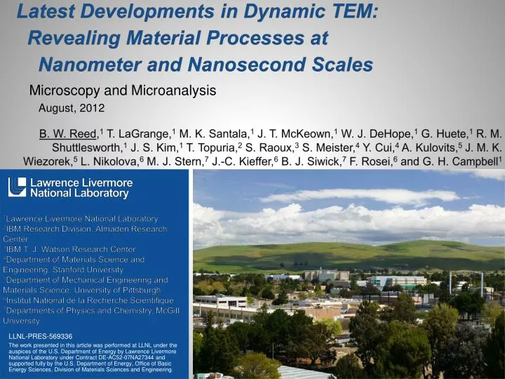
Latest Developments in Dynamic TEM: Revealing Material Processes at Nanometer and Nanosecond Scales. Microscopy and Microanalysis. August, 2012.

E N D
Latest Developments in Dynamic TEM: Revealing Material Processes at Nanometer and Nanosecond Scales Microscopy and Microanalysis • August, 2012 B. W. Reed,1 T. LaGrange,1 M. K. Santala,1 J. T. McKeown,1 W. J. DeHope,1 G. Huete,1R. M. Shuttlesworth,1 J. S. Kim,1 T. Topuria,2 S. Raoux,3 S. Meister,4 Y. Cui,4 A. Kulovits,5J. M. K. Wiezorek,5 L. Nikolova,6 M. J. Stern,7 J.-C. Kieffer,6 B. J. Siwick,7 F. Rosei,6 and G. H. Campbell1 1Lawrence Livermore National Laboratory 2IBM Research Division, Almaden Research Center 3IBM T. J. Watson Research Center 4Department of Materials Science and Engineering, Stanford University 5Department of Mechanical Engineering and Materials Science, University of Pittsburgh 6Institut National de la RechercheScientifique 7Departments of Physics and Chemistry, McGill University
Single-Shot Dynamic TEM (DTEM) is aimed at solving problems in materials science . . . Laser-pulse driven photoelectron cathode For materials science, in situ TEM is often concerned with: • Microstructural evolution • Phase transformations • Chemical reactions involving nanostructured materials • Damage e-s Cathode drive laser Nd:YLF (5w) l = 211nm 10 ns FWHM pulse width Probe e-s • Sample drive laser • Nd:YAG • = 1064nm or 355nm 12 ns FWHM pulse width Sample Location Beam Shifter e-s In most applications, these things never unfold exactly the same way twice CCD Camera
. . . yet what you really want is to capture not a single shot but a movie. Nucleation and growth of a single crystalline grain in laser-heated amorphous GeTe This is not a montage of individual experiments This is a set of nine TEM images captured in under 3 µs
The Arbitrary Waveform Generation (AWG) Laser can produce temporally shaped laser pulses over an unprecedented temporal range with high spatial mode quality and energy. • Produces variable pulse widths from 5 ns to 10 µs and pulse trains in 250µs temporal window • Designed to deliver energies up to 1 J per pulse for high photoelectron yield after UV conversion • Fiber-based optical components, solid-state diode amplifiers and adaptive optics provide high stability and beam quality
Movie Mode works by synchronizing an arbitrary series of laser pulses with a fast post-sample deflector
Movie Mode works by synchronizing an arbitrary series of laser pulses with a fast post-sample deflector Pulse Train of Electrons 9 electron pulses with temporal resolution from 5ns to 10s and interframe times from 25ns to 250s AWG cathode laser generates a UV pulse train High Voltage Electrostatic Deflector rasters pulse train onto the CCD Sample drive laser 1 pulse or drive event Electrostatic Deflector 2k x 2k Single-electron Sensitive CCD camera The CCD is read out at the end of experiment and segmented into frames.
The images are rastered in two dimensions What the camera sees How it's interpreted
The system is extremely programmable and can potentially operate in many different modes • The laser itself can have essentially any temporal profile, subject to: • ~5 ns resolution • ~250 µs total run time (with some limits) • ~1 J total • The electrostatic deflectors can be made to operate in any sequence at all, switching on and off arbitrarily • This includes switching during an electron pulse for streaking • And of course all the usual TEM imaging and diffraction modes are available, along with in situ sample holders • Novel methods of driving the sample, beyond just a laser pulse, are of interest • The AWG laser may also be used as a sample drive laser
Example Application: Metastable phase transformations in Ge2Sb2Te5 (GST) • Laser amorphization in Ge2Sb2Te5 takes ~10ns, laser crystallization ~100ns • Amorphization requires very rapid quenching, ~1010 K/s • Time-resolved crystallization experiments performed on amorphous films • In situ laser switching achieved by use of a novel specimen geometry crystalline amorphous amorphous crystalline time Laser power higher power amorphizing pulse lower power crystallizing pulse
Phase change materials: Ge2Sb2Te5 crystallization 002 111 Time-resolved crystallization 022 111 002 022 • As-deposited amorphous Ge2Sb2Te5 films were laser crystallized • Various time-delays recorded • Rotationally averaged data used to map out the time to crystallization 222 133 024 224 113 004 microcrystalline Intensity (arbitrary units) 50 ns delay curves offset for visibility amorphous 4 8 12 Santala et al. J. Appl.Phys. 111 (2012) k (nm-1)
Movie mode reveals previously invisible details of nucleation, growth, and impingement How fast is the nucleation? When does it happen? How fast does the front move? When do stresses start to become important? How does the evolution change after impingement? Why is the microstructure nonuniform at the end? All these questions can now be answered directly.
Example application: Crystallization of amorphous germanium yields three zones of differing crystalline morphology Conventional TEM image of laser crystallized area of a-Ge film Zone III: Layers of elongated grains oriented circumferentially and nanocrystals a-Ge Zone II: Elongated radial grains Zone I: Nanocrystalline 5 μm
Example application: Development of microstructure in laser melt and resolidification of metallic thin films Liquid Laser Irradiation Nanocrystalline Microcrystalline Liquid unmelted Before During After Si Substrate SiO2 Capping Layer We can observe morphological changes in liquid-solid interface of rapid lateral solidification (RLS) of molten metal films and quantitatively measure interface velocities (e.g., images show a planar front moving at ~3.5 m/s). Al -Metal SixNy Membrane
Rapid Alloy Solidification: Al-7 at.% Cu Time-resolved imaging reveals the evolution of the microstructure as the melted film re-solidifies As-deposited 15 µs 20 µs As-deposited 25 µs 30 µs Re-solidified As-deposited films are nanocrystalline and ~80 nm thick
Rapid Alloy Solidification: Al-7 at.% Cu Region 1: Small Al-rich Grains Regions 2 and 3: Large Columnar and Interior Grains • There are 3 morphologies produced in the the film by laser irradiation: • Small Al-rich grains with Cu segregated to the grain boundaries • Large columnar grains with [100] cube-direction growth axes • Columnar grains produce two large interior grains and multiple “wraparound” grains [200] Dark-field STEM image EDS Cu Map [200]
Rapid Alloy Solidification: Effects of Cu Content 20 µs 25 µs Re-solidified Effects of Increasing Cu Content • Time-resolved imaging shows, with increasing Cu content: • Increased times for the alloy to solidify • A more jagged solid/liquid interface • A shrinking columnar region • Increasing number of interior grains 7 at. % Cu 30 µs 40 µs Re-solidified 12 at. % Cu 50 µs 60 µs Re-solidified 18 at. % Cu (Eutectic)
Example Application: Reactive multilayer foils (RMLF) 1 mm 1 mm Reacted Foil Laser spot Reaction Zone Atomic Diffusion Atomic Mixing 14.6 ms after drive initiation Thermal Diffusion 50 mm ~13 m/s (nm/ns) Propagation Unreacted Foil Cross section Plan view Unreacted foil Ni Al Intermetallic Reacted foil NiAl –B2 intermetallic Laser • Advantages of DTEM studies: • Conventionally, direct metastable state observations at the nanoscale cannot be done • Past studies have only used electron microscopy on quenched RMLFs Electron Pulse
2 Al : 3 NiV 3 Al : 2 NiV 3 mm 8 mm Off-equiatomic compositions produce short-lived striations behind the reaction front The 3 Al:2 NiV foils have a shorter region of transient morphology and smaller periodicity than those grown at 2 Al:3 NiV The observed Al loss in Al-rich samples from surface evaporation may result in the rapid quenching of the sample and explain the shorter length
2 Al : 3 NiV 3 mm 3 Al : 2 NiV 1 Al : 1 NiV 3 mm 3 mm A very likely interpretation is that the striations are liquid The estimated temperature rise from an adiabatic calculation is ~100K below the congruent melting point
With the Movie-mode capability, we can directly follow rapid phase transitions and morphological changes at the reaction front
Similarly, in Ti-B multilayer foils, we have observed a thin transient zone behind the reaction front that could contain multiple phases Dark-contrast regions between grains have been observed in a zone roughly 3-4μm in size behind the propagating front. Liquid? This transient zone may be two-phase as in the NiAl system, containing TiB2 in both solid and liquid phases. 1 μm
We have observed the phase transitions with time-resolved electron diffraction in a 1.75 µm region at the propagating reaction front The Ti-B RMLF transforms from nc-Ti/a-B layered structure to nc-TiB2 within 625ns. This implies an extremely high cooling rate.
Movie Mode Dynamic TEM has arrived.Where do we go from here? • Tweak the system for better performance • Re-engineer the gun for better brightness • Understand the real resolution limits. How bad is stochastic blur? What about damage? • Develop new operating modes based on this technology • Integrate in situ sample holders and sample drives • Integrate with advanced detectors And of course, now that the capability exists, • Do the best dynamic materials science that we can! Capture the crucial in between moments that have never been seen before.
To calibrate models on reactive powder compacts, we are studying reaction dynamics in Ti-B RMLFs • Three foil compositions: Ti-2B, 2Ti-3B and 3Ti-2B. • Films are capped with Tiand have 6.5 bilayers with a 39nm bilayer thickness, giving a 250nm total thickness • Reaction front propagates at 13.2 ± 0.1m/s • Adiabatic heat rise (~3500K) suggests melting of both layers near front (Z.A. MunirAm. Ceram. Soc. Bull.67, 342 (1988)) • Observed Ti loss suggests that evaporative cooling may be important Work in Collaboration with David Adams at SNL Albuquerque