Graphene oxidation
Graphene oxidation. Graphene oxidation is used to create a single layer graphene sheet. Graphene layers produced Oxidation experimental procedure. Sample oxidized at 450 o C for 10 min; Sample heated at 550 o C for 10 min; Sample heated at 550 o C for 20 min;

Graphene oxidation
E N D
Presentation Transcript
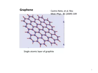
Graphene oxidation Graphene oxidation is used to create a single layer graphene sheet.
Graphene layers producedOxidation experimental procedure • Sample oxidized at 450 oC for 10 min; • Sample heated at 550 oC for 10 min; • Sample heated at 550 oC for 20 min; Atomic force microscopy (AFM) after each step to see the effects of the oxidation on several graphite platelets AFM use Nanoscope IIIa instrument operating in air.
AFM of graphite platelet • Platelet folds in several surfaces • Nanoparticles on a surface • Surface roughness (RMS) –> flattening; • Height of platelet
AFM cont. • Height decrease from 2.9 nm to 0.7-1.1 nm due to removal of residual material • Monoleyer dips began to appear
AFM cont. • c.11’ – single graphene layer (0.39nm) • 22 – two-layer thickness • d. 11’-Thickness becomes uniform • 22’ – etched substrate surface (SiO2 layer) (0.4nm)
4th oxidation step • 550 oC for 30 min. • Armchair edge
Electronic properties • Depend on the width; • Edge effects; • Band structure observed by scanning tunnelling microscopy and spectroscopy
Optical properties • Raman spectroscopy: • thickness (layer no) 2D/G; • Disorder (lattice defects) D/G; • Temperature • Sensitive to a single layer
Conclusion • Graphene single layers bring interest in nanoscience • Building blocks in electronic applications; • Graphene transistor • Graphite oxidation paper