Download
1 / 16
160 likes | 377 Views
Fast Electronics of T0 Detector. Anatoly.Klimov@cern.ch 10 December 2004. Placement of T0 fast electronics. The electronic equipment (fast electronics) is assumed to be placed in VME crates and located in experimental area at the outer side of the L3 magnet.

E N D
Fast Electronicsof T0 Detector Anatoly.Klimov@cern.ch 10 December 2004
Placement of T0 fast electronics The electronic equipment (fast electronics) is assumed to be placed in VME crates and located in experimental area at the outer side of the L3 magnet.
Electronics equipment carries out three basic functions: • Realization of the logic selection allowing considerably to lower a level of background events at development of trigger signals TO; • Generation of signals, with precision accuracy fixing time marks of occurrence of pulses; • Measurement of the amplitude and time distributions of the signals of the detectors.
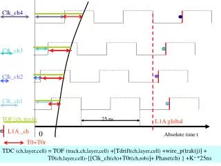
The overall diagram of T0 fast electronics Signals from shoeboxes go to analog splitters and further to QTC, CFD– discriminators and multiplicity discriminators. The output pulses of the CFD – discriminators through lines of a delay go to 12 channel circuits of coincidences (OR) for generation of signals TO-A, TO-C. Output pulses of QTC and CFD – discriminators go to TRM (TDC Readout Module) for conversion and the subsequent transfer in DAQ (Detector Acquisition System). Output pulses of multiplicity discriminators, circuits of coincidence (OR) and the block of time discrimination (TVDC) through NRZ module are transferred in CTP (Central Trigger Processor).
T0 Vertex Unit (TVDC) • TVDC should meet the following requirements: • range of conversion time intervals: 2,5 ns(5 ns); • quantization step: 20 ps (for 8-bit conversion); • dead time of conversion: not more than 25 ns. TVDC is in CAMAC standard The given parameters obtained with the use of time-amplitude converter and flash ADC with the digital discriminator for TO-vertex signal generation.
Threshold characteristic of TVDC Measured at the CERN accelerator PMT position 2(shift = 18 cm) The duration of delay slope is determined by the real resolution (FWHM) of the detectors used in the experiment PMT position 1
TVDC calibration tests TVDC calibration spectrum • Calibration spectrum derived from the 0.5 ns discrete change of delay between start and stop pulse • Peak distance is 23 channels • The time resolution of TVDC is around 22 ps
Multiplicity Discriminator (MPD) • MPD generates three logical signals corresponding to three levels of multiplicity: • Low(minimum bias) • Intermediate (semi–central) • High(central) The multiplicity level is adjusted discretely (8-bit) MPD is in CAMAC standard Pulse shape of the anode of the PMT Parameters: • Number of inputs: 12 • Maximum amplitude of the signal at each input: 3 V. • Minimal duration: 5 ns. • Rise time: 2.5 ns • The output signal at the Out1-Out3 outputs is in the NIM standard with the 10 ns duration
MPD linearity tests QDC doesn’t start analyze incoming amplitude signals until MPD produce ‘Strobe’ signal Emulation of multiplicity of PMT output signals
Other units (CFD, Mean Timer, Delay Unit, Logical Unit etc.) have prototypes but need further development and tuning. All electronics units was made in CAMAC standard. It is necessary to develop this units in VME standard.
VME interface Functional part of CAMAC units It suggested to place FE units on 6U VME boards and use universal VME decoder. VME Board
FPGA XILINX XC9500 • Features • High-performance • 5 ns pin-to-pin logic delays on all pins • fCNT to 125 MHz • Endurance of 10,000 program/erase cycles • Global and product term clocks, output enables, set and reset signals • Extensive IEEE Std 1149.1 boundary-scan (JTAG) support • High-drive 24 mA outputs • 3.3V or 5V I/O capability • Advanced CMOS 5V Fast FLASH™ technology • Supports parallel programming of multiple XC9500 devices
Wiener VME 5021 Crate • 19" VME bins: • 8U or 9U bin for 6U x 160mm VME cards • 21 slots • 2U space for fan tray • Various backplanes possible: standard J1/J2, CERN-V430 J1/J2/Jaux, VME 64 • Equipped with multiple high current connector board
VME Power Supply UEP 5021 • Mains filter • Softstart circuit • Auxiliary power supply • Regulator-monitoring- and alarm-circuit supported by a self calibrating microprocessor system.
FE modules arrangement Controlled by V2718 Without control 2 VME crates 6 Delays (4-ch. each) 2 ORs 2 MPDs 1 TVDC 6 QTCs (4-ch. each) 6 FAN-OUTs (4-ch. each) 12 CFDs (2-ch. each) 1 TM 1 NRZModule 17 modules 20 modules
Problems It is necessary to: develop prototype of QTC and NRZ module develop system of time synchronization (BC) for FE units develop system of laser calibration for detector T0 choose appropriate CFD for precision time measurement make uniform interfaces of DAQ and DCS