Download
1 / 54
550 likes | 779 Views
2.2 MSP430 Microarchitecture. Required : PM : Ch 4, pgs 37-46-127 PM : Ch 8.1-3, pgs 109-114 Recommended : Wiki : Microarchitecture Wiki : Addressing_mode Wiki : Three-state logic. Learning Objectives….

E N D
2.2 MSP430 Microarchitecture Required: PM: Ch 4, pgs 37-46-127 PM: Ch 8.1-3, pgs 109-114Recommended: Wiki: MicroarchitectureWiki: Addressing_modeWiki: Three-state logic
Learning Objectives… After discussing microarchitecture and studying the reading assignments, you should be able to: • Explain what is a computer microarchitecture. • Describe how memory-mapped I/O is implemented. • Program digital I/O using computer ports. • List the addressing modes of the MSP430. • Identify MSP430 microarchitecture components. • Explain how a microarchitecture executes computer instructions. • Identify multiplexor, decoder, driver, ALU, and register circuitry. • Explain program counter, stack pointer, and condition code registers. • Explain the difference between clock cycles and instruction steps. MSP430 Microarchitecture
Terms… • Absolute Addressing – direct addressing of memory (immutable). • Address Space– number of addressable memory locations. • Addressability – size of smallest addressable memory location. • Arithmetic Logic Unit (ALU) – combinational logic that performs arithmetic and logical operations. • Bus– physical connection shared by multiple hardware components. • Finite State Machine – finite set of states than transition from a current to next state by some triggering condition. • Indexed Addressing – final address is offset added to base address. • Instruction Phases– steps used by a FSM to execute an instruction. • Memory Mapped I/O– memory locations used to input/output. • Microarchitecture – physical implementation of an ISA. • Read-Before-Write – access memory before changing with write. • Relative Addressing– address is relative to current memory position. MSP430 Microarchitecture
Bits A[15:9] Memory Mapped I/O Memory Mapped I/O Memory Address Bus (A[15:0]) ... 512 Peripherals ... 9 to 512 Decoder Bits A[8:0] Device 0x01fe Device 0x0000 Device 0x01ff High (1) if and only if bits 9-15 are low (0). High (1) if any of bits 9-15 are high (1). Memory CS MSP430 Microarchitecture
Memory Mapped I/O MSP430 P1/P2 Port Registers 0xFFFF • Memory Mapped I/O • 8 bit memory locations • Each bit independently programmable for I/O • Edge-selectable input interrupt capability (P1/P2) • Individually programmable pull-up/pull-down resistors bis.b #0x0f,&P1DIR bis.b #0x0f,&P1OUT • xor.b#0x0e,&P1OUT 0000 1111 0x0000 0000 0001 0000 1111 MSP430 Microarchitecture
Memory Mapped I/O Digital Port Input/Output • Direction Register (PxDIR): • Bit = 0: the individual port pin is set as an input (default) • Bit = 1: the individual port pin is set as an output • Input Register (PxIN): • Bit = 1: The input port pin is high • Bit = 0: The input port pin is low • Output Register (PxOUT): • Bit = 1: The output port pin is set high; • Bit = 0: The output port pin is set low. • Note: the PxOUT is a read-write register which means previously written values can be read, modified, and written back MSP430 Microarchitecture
LaunchPad Ports LEDs • LaunchPadDevelopment Tool • P1.0 Red LED • P1.6 Green LED • Example bis.b #0x41,&P1DIR; P1.0,P1.6 output bic.b #0x01,&P1OUT; turn off red LED bis.b #0x40,&P1OUT; turn on green LED xor.b #0x41,&P1OUT; toggle LEDs MSP430 Microarchitecture
Quiz 2.2.1 Four LEDs are attached to Port 1, bits 0 thru 3. Indicate which LEDs are ON/OFF/Undefined after each instruction to the left is executed. P1.3 P1.2 P1.1 P1.0 • mov.b #0x0f,&P1DIR • and.b #0xf0,&P1OUT • bis.b #0x09,&P1OUT • xor.b #0x0f,&P1OUT • bic.b #0x06,&P1OUT • add.b #0x03,&P1OUT MSP430 Microarchitecture
ISA a b NOR Finite State Machine A B Storage Devices we d S d q Register we Register we we 2-to-4 Decoder 4-to 1 Multiplexor q Register q we Register C we Sequential Logic W A B a1 a0 X Y Z Combinational Logic Complementary Logic Transistor Microarchitecture Microarchitecture Journey Microarchitecture MSP430 Microarchitecture
Microarchitecture Microarchitecture • The Instruction Set Architecture (ISA) defines the processor instruction set, processor registers, address and data formats • The processor as seen by an assembly language programmer. • The microarchitecture implements the ISA. • Gates, registers, ALUs, clocks • Data and control paths • Microarchitectures differentiate themselves by: • Chip area/cost • Power consumption • Logic complexity • Manufacturability • Ease of debugging • Testability MSP430 Microarchitecture
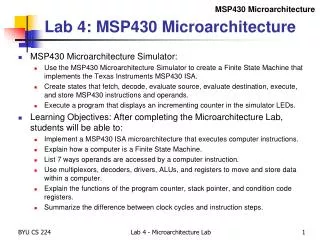
MSP430 Microarchitecture Lab 4: MSP430 Microarchitecture • MSP430 Microarchitecture Simulator: • Use the MSP430 Microarchitecture Simulator to create a machine that implements the Texas Instruments MSP430 ISA. • Generate a Finite State Machine (FSM) for fetch, decode, evaluate source, evaluate destination, execute, and store cycles of MSP430 instructions. • Execute a program that displays an incrementing counter in the simulator LEDs. • Learning Objectives: • Learn how a microarchitecture executes computer instructions. • Learn about multiplexor, decoder, driver, ALU, and register circuitry. • Learn about program counter, stack pointer, and condition code registers. • Understand better the difference between clock cycles and instruction steps. Lab 4 - Microarchitecture Lab
MSP430 Microarchitecture MSP430 Machine Code ;************************************************************** ; MSP430 Micro-Architecture Simulator Code ; ; Description: Display an incrementing counter in LEDs. ;************************************************************** .cdeclsC,"msp430.h" .text 8000: 4031 0300 RESET: mov.w #0x0300,SP ; Initstack pointer 8004: 40b2 5a80 0120 mov.w #WDTPW+WDTHOLD,&WDTCTL ; Stop WDT 800a: d0f2 000f 0022 bis.b#0x0f,&P1DIR ; Set P1.0-3 output 8010: 430e mov.w #0,r14 8012: 4ec2 0021 loop: mov.b r14,&P1OUT ; output P1.0-3 8016: 531e add.w #1,r14 8018: f03e 000f and.w #0x000f,r14 ; mask counter 801c: 401f 0003 mov.w delay,r15 ; Delay to R15 8020: 120f push r15 8022: 8391 0000 wait: sub.w #1,0(sp) ; decrement delay count 8026: 23fd jnz wait ; delay over? 8028: 41ef mov.w @sp+,r15 ; y 802a: 3ff3 jmp loop ; repeat 802c: 0002 delay: .word 2 .sect ".reset" ; MSP430 RESET Vector .word RESET ; NMI .end Lab 4 - Microarchitecture Lab
MSP430 Microarchitecture MSP430 Microarchitecture Simulator Lab 4 - Microarchitecture Lab
MSP430 Clock Cycles MSP430 InstructionCycles • Data being sent/received on the data bus is called a cycle. • 1 cycle to fetch instruction word • +1 cycle if source is @Rn, @Rn+, or #Imm • +2 cycles if source uses indexed mode • 1st to fetch base address • 2nd to fetch source • Includes absolute and symbolic modes • +2 cycles if destination uses indexed mode • +1 cycle if writing destination back to memory • Additionally • +1 cycle if writing to PC (R0) • Jump instructions are always 2 cycles MSP430 Microarchitecture
Quiz 2.2.2 • Given a 1.2 MHz processor, what value for DELAY would result in a 1/4 second delay? ? DELAY .equ mov.w #DELAY,r12 ; 2 cycles delay1: mov.w #1000,r15 ; 2 cycles delay2: sub.w #1,r15 ; 1 cycle jne delay2 ; 2 cycles sub.w #1,r12 ; 1 cycle jne delay1 ; 2 cycles MSP430 Microarchitecture
MSP430 Microarchitecture MSP430 Microarchitecture Memory (Address Space) Control Logic (Finite State Machine) Clocks ALU Input/Output MSP430 MPU 16 16-bit Registers MSP430 Microarchitecture
Quiz 2.2.3 • ALU • Clocks • Control • I/O • Memory • Peripherals • Registers • Address space • Execution speed • External devices • Fast memory • Finite State Machine • Memory mapped • Word length • Match the following terms: MSP430 Microarchitecture
Instruction Cycle The Instruction Cycle • INSTRUCTION FETCH • Obtain the next instruction from memory • DECODE • Examine the instruction, and determine how to execute it • SOURCE OPERAND FETCH • Load source operand • DESTINATION OPERAND FETCH • Load destination operand • EXECUTE • Carry out the execution of the instruction • STORE RESULT • Store the result in the designated destination Not all instructions require all six phases MSP430 Microarchitecture
PC Fetch Cycle Fetching an Instruction PC can be incremented anytime during the Fetch phase MSP430 Microarchitecture
Addressing Modes The MSP430 has four basic addressing modes: 00 = Rs - Register 01 = x(Rs) - Indexed Register 10 = @Rs - Register Indirect (source only) 11 = @Rs+ - Indirect Auto-increment(source only) When used in combination with registers R0-R3, three additional source addressing modes are available: label - PC Relative, x(PC) &label – Absolute, x(SR) #n – Immediate, @PC+ (source only) Addressing Modes MSP430 Microarchitecture
Quiz 2.2.4 • add.w tab(r10),r9 • and.w &mask,r12 • bis.b #0x08,r6 • mov.b cnt,r11 • mov.w r4,r5 • mov.w #100,r14 • sub.w @r4+,r5 • xor.b @r8,r15 • Absolute • Constant • Immediate • Indexed register • Indirect auto-increment • Indirect register • Register • Symbolic • Match the following source operand modes: MSP430 Microarchitecture
Addressing Modes Addressing Mode Demo 8000: 540A 8002: 541A 0006 8006: 542A 8008: 543A 800a: 501A 0012 800e: 521A 801e 8012: 503A 0064 8016: 531A 8018: 1210 0004 801c: 3ff1 801e: 000a .text start: add.w r4,r10 ; r4 += r10; add.w 6(r4),r10 ; r10 += M[r4+6]; add.w @r4,r10 ; r10 += M[r4]; add.w @r4+,r10 ; r10 += M[r4++]; add.w cnt,r10 ; r10 += cnt; add.w &cnt,r10 ; r10 += cnt; add.w #100,r10 ; r10 += 100; add.w #1,r10 ; r10++; push cnt ; M[--r1] = cnt; jmp start cnt: .word 0x000a MSP430 Microarchitecture
00 = Register Mode Addressing Modes add.w r4,r10 ; r10 += r4 Address Bus Memory CPU Registers Data Bus (1 cycle) IR 0x540a +2 PC PC 0x540a ADDER PC R4 R10 ALU MSP430 Microarchitecture
Rs Evaluate Source Operand Source: Register Mode – Rs Select the source register MSP430 Microarchitecture
01 = Indexed Mode Addressing Modes add.w 6(r4),r10 ; r10 += M[r4+6] Address Bus Memory CPU Registers Data Bus (1 cycle) IR 0x541a +2 +2 PC PC PC 0x541a ADDER PC 0x0006 Data Bus (+1 cycle) R4 Address Bus R10 Data Bus (+1 cycle) ALU MSP430 Microarchitecture
Rs PC PC Evaluate Source Operand Source: Indexed Mode – x(Rs) PC incremented at end of phase Use PC to obtain index, use Rs for base register MSP430 Microarchitecture
10 = Indirect Register Mode Addressing Modes add.w @r4,r10 ; r10 = M[r4] Address Bus Memory CPU Registers Data Bus (1 cycle) IR 0x542a +2 PC PC 0x542a ADDER PC R4 Address Bus R10 Data Bus (+1 cycle) ALU MSP430 Microarchitecture
Rs Evaluate Source Operand Source: Indirect Mode – @Rs MSP430 Microarchitecture
Addressing Modes 11 = Indirect Auto-increment Mode add.w @r4+,r10 ; r10 += M[r4++] Address Bus Memory CPU Registers Data Bus (1 cycle) IR 0x543a +2 PC PC 0x543a ADDER PC 0002 Address Bus R4 R10 Data Bus (+1 cycle) ALU MSP430 Microarchitecture
Source: Indirect Auto Mode – @Rs+ Rs Evaluate Source Operand Increment by 1 (.b) or 2 (.w) MSP430 Microarchitecture
Addressing Modes 01 w/R0 = Symbolic Mode add.w cnt,r10 ; r10 += M[cnt] Address Bus Memory CPU Registers Data Bus (1 cycle) IR 0x501a +2 +2 PC PC PC PC 0x501a ADDER PC 0x000c Data Bus (+1 cycle) Address Bus cnt R10 Data Bus (+1 cycle) ALU *Also called PC Relative address mode MSP430 Microarchitecture
PC PC PC Evaluate Source Operand Source: Symbolic Mode – label PC incremented at end of phase Use PC to obtain relative index and for base register MSP430 Microarchitecture
Quiz 2.2.5 Present the destination operand of the following instruction to the ALU: add.w r4,cnt ; M[cnt] += r4 Memory CPU PC PC PC PC ADDER Registers IR 0x5480 PC 0x5480 0x0218 R4 cnt ALU MSP430 Microarchitecture
Addressing Modes 01 w/R2 = Absolute Mode add.w &cnt,r10 ; r10 += M[cnt] Address Bus Memory CPU Registers Data Bus (1 cycle) IR 0x521a +2 +2 PC PC PC 0x521a ADDER PC 0xc018 Data Bus (+1 cycle) 0000 Address Bus cnt R10 Data Bus (+1 cycle) ALU MSP430 Microarchitecture
Source: Absolute Mode – &Address #0 PC Evaluate Source Operand PC can be incremented anytime during the phase Use PC to obtain absolute address, use #0 for base register MSP430 Microarchitecture
Addressing Modes 11 w/R0 = Immediate Mode add.w #100,r10 ; r10 += 0x0064 Address Bus Memory CPU Registers Data Bus (1 cycle) IR 0x503a +2 +2 PC PC PC 0x503a ADDER PC 0x0064 Data Bus (+1 cycle) R10 ALU MSP430 Microarchitecture
PC Evaluate Source Operand Source: Immediate Mode – #n PC can be incremented anytime during the phase MSP430 Microarchitecture
MSP430 Source Constants To improve code efficiency, the MSP430 "hardwires" six register/addressing mode combinations to commonly used source values: #0 - R3 in register mode (00) #1 - R3 in indexed mode (01) #2 - R3 in indirect mode (10) #-1 - R3 in indirect auto-increment mode (11) #4 - R2 in indirect mode (10) #8 - R2 in indirect auto-increment mode (11) Eliminates the need to use a memory location for the immediate value - commonly reduces code size by 30%. Evaluate Source Operand MSP430 Microarchitecture
Addressing Modes Constant Generator add.w #1,r10 ; r10 += 1 Address Bus Memory CPU Registers Data Bus (1 cycle) IR 0x531a +2 PC PC 0x531a ADDER PC 0000 0001 0002 0004 0008 ffff R10 ALU MSP430 Microarchitecture
Constant Mode – #{-1,0,1,2,4,8} R3 Evaluate Source Operand MSP430 Microarchitecture
Addressing Modes 3 Word Instruction add.wcnt,var ; M[var] += M[cnt] Address Bus Memory CPU Registers Data Bus (1 cycle) IR 0x5090 +2 +2 +2 PC PC PC PC 0x5090 ADDER PC PC 0x000c Data Bus (+1 cycle) 0x0218 Data Bus (+1 cycle) Address Bus cnt Data Bus (+1 cycle) Address Bus var ALU Data Bus (+1 cycle) Data Bus (+1 cycle) MSP430 Microarchitecture
Quiz 2.2.6 Show how to retrieve a PC-relative destination operand from memory and present to the ALU: MSP430 Microarchitecture
Final Instruction Phases • Execute • PUSH • Decrement stack pointer (R1) • Ready address for store phase • JUMP • Compute 10-bit, 2’s complement, sign extended • Add to program counter (R0) • Store • Move data from ALU to register, memory, or I/O port MSP430 Microarchitecture
Execute Phase Push Instruction push.wcnt ; M[--sp] = M[cnt] Address Bus Memory CPU Registers Data Bus (1 cycle) IR 0x1210 +2 +2 PC SP PC SP PC PC 0x1210 ADDER PC fffe 0x000c SP Data Bus (+1 cycle) (+1 cycle) Address Bus cnt 0xa5a5 Data Bus (+1 cycle) Address Bus 0xa5a5 ALU Data Bus (+1 cycle) MSP430 Microarchitecture
Execute Phase: PUSH.W SP Use Store Phase to push on stack Execute Cycle SP = SP - 2 MSP430 Microarchitecture
Addressing Modes Execute Phase: jnefunc jnefunc ; pc += sext(IR[9:0]) << 1 Address Bus Memory CPU Registers Data Bus (1 cycle) IR 0x3c2a +2 PC PC 0x3c21 ADDER PC SEXT[9:0]<<1 R2 Jump Next COND func ALU MSP430 Microarchitecture