Download
1 / 56
590 likes | 868 Views
Design and Modeling of RF Circuits using Design of Experiments. VLSI Consortium workshop 29 Oct. 2010. Jai Narayan Tripathi / Jayanta Mukherjee Department of Electrical Engineering IIT Bombay, Mumbai 400076, INDIA. Agenda.

E N D
Design and Modeling of RF Circuits using Design of Experiments VLSI Consortium workshop 29 Oct. 2010 Jai NarayanTripathi / JayantaMukherjee Department of Electrical Engineering IIT Bombay, Mumbai 400076, INDIA.
Agenda • Challenges in RF Circuit Design - Design Challenges - Modeling Challenges • Introduction to DOE • Robust Optimization and ANOVA. • Final Design of Oscillator • Case study 1 : Improving Signal Integrity - Statistical Analysis - Optimization - Results • Case study 2 : DesigningLow Phase Noise Oscillator • Work in progress - Improving Accuracy in Modeling • Future Work - Phase Noise Modeling of Ring Oscillator
Objectives • To apply DOE to RF active circuits, to improve and model their output characteristics. • To develop systematic approach of circuit design/modeling, using Robust Design approach.
Design Challenges : CMOS Differential LC Oscillator • Generally used as an Local Oscillator (LO). • Desired frequency can be achieved by setting L and C. • As the oscillation frequency increases, phase noise decreases. • How to design at a particular frequency with minimum phase noise ??? - as phase noise will be set lower, frequency will change !!!
Designing Low Phase Noise Oscillator • Designing a CMOS differential LC tank oscillator with minimum phase noise. • The library used is UMC 180 nm rf lib. • The design variables are : - Finger number of transistors, - Inductor top metal width, - Inductor inner diameter, - Length of unit square of capacitor, and - Width of unit square of capacitor. • Importance of Phase Noise ? - QoS of communication is characterized by Phase Noise. - Transceivers have more probability of interference. - SNR of a communication system may get affected.
Design Variables (Physical) or Control Factors for DOE • 1) Width of Transistor M1 (Finger no. w1) • 2) Width of Transistor M2 (Finger no. w2) • 3) Width of Transistor M3 (Finger no. w3) • 4) Width of Transistor M4 (Finger no. w4) • 5) Width of Transistor M5 (Finger no. w5) • 6) Width of finger of Inductor (w6) • 7) Width of Capacitor (w7) • 8) Diameter of finger of Inductor (d) • 9) Length of Capacitor (l)
Quality Engineering • “Quality Engineering” is a branch of engineering that deals with the yield and the quality of the production. • DOE techniques are used for Robust Optimization of an RF Oscillator. • For Orthogonal Experiments, Taguchi Methods are used to optimize the system.
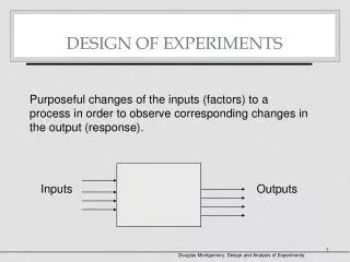
Design Of Experiments (DOE) • Method to efficiently design a system to maintain it’s important output parameters within the robustness limits of the functionality of the system [5]. 1) Full Factorial Experiments: It considers all the possible combinations and based on the results, optimization is performed. E.g. in our circuit there will be 2*(3)^7 = 4374 experiments.
2) Fractional Factorials : • This method facilitates to perform only certain combinations out of all the possible combinations. • The set of experiments can be defined either by an orthogonal array, or by forming a subgroup of the direct product of Abelian groups of orders equal to the number of levels of each factor [6].
In our case, we are performing 50 certain combinations i.e. experiments, instead of about 1.9 million experiments. • These combinations are taken according to Orthogonal Array (L50). • For 9 parameters, the available table is L50(2^1, 5^11). • Orthogonal Arrays provide best possible information in least no. of simulations.
Analysis of Variance • It is also called ANOVA. • ANOVA can find out the % contribution of each factor for the output quality parameter. • Consider a set of n experiments with k design factors -
In ANOVA, mean of all the responses is calculated. Based on the variance of each response from the mean, the variance contributed by each factor is calculated. • By ANOVA, % effect of each factor can also be calculated. • Additive Model for factor effects
Robust Optimization • Robust optimization means to optimize a design in such a way that it will certainly work according to the specifications for which it is desired to work. • Robust Optimization assures the proper functioning of the system.
Taguchi optimization of Active Circuits • DOE are widely used in electronic industry for getting better yields [1]. • Literature is available for the same, but most of them talk about passive circuit optimization or device optimization [2-4]. • This is an attempt to optimize active circuits using DOE and Taguchi methods.
Case Study 1 : Improving Eye Diagram of RF Oscillator • Signal Integrity ensures reliable transmission at higher speeds. • Oscillators are generally used in transceivers, where we need good SI because the received signal is already distorted. • The main concern is to improve Eye Diagram.
Design Parameters and their Levels • 1) Width of Transistor M1 (Finger no. w1) • 2) Width of Transistor M2 (Finger no. w2) • 3) Width of Transistor M3 (Finger no. w3) • 4) Width of Transistor M4 (Finger no. w4) • 5) Width of Transistor M5 (Finger no. w5) • 6) Width of finger of Inductor (w6) • 7) Width of Capacitor (w7) • 8) Diameter of finger of Inductor (d)
Sensitivity coefficients vectors calculated from Ordinary Least Square (OLS) methods
Linear additive models after replacing sensitivity coefficients
Results and Remarks • Jitter is about 158 psec (130%) reduced. • Eye Height is 1.12 V increased. • In addition of that, SNR is increased by • almost 87%. • Power consumption of optimized design is • 16.93 mW compared to 17.67 mW of • standard design.
Case Study 2 : Designing Low Phase Noise 2 GHz Oscillator • The main concern is to reduce phase noise with minimum deviation in frequency of oscillation.
Design Parameters and their Levels • 1) Width of transistor M1 (Finger no. w1) • 2) Width of transistor M2 (Finger no. w2) • 3) Width of transistor M3 (Finger no. w3) • 4) Width of transistor M4 (Finger no. w4) • 5) Width of transistor M5 (Finger no. w5) • 6) Width of finger of Inductor (w6) • 7) Width of unit square of capacitor (w7) • 8) Diameter of finger of inductor (d) • 9) Length of unit square of capacitor (l)
The same set of experiments was performed at following temperatures : • 1. 15oC • 2. 25oC • 3. 35oC • 4. 45oC • 5. 55oC
ANOVA • This is the case of “smaller the better” for phase noise. • All the simulation results are converted in to their logarithmic values (dB). • The overall mean is -36.27 dB. • Effect of ‘w7’ and ‘l’ on phase noise are 46% and 45% respectively. • Effect of ‘d’ on phase noise is 2% but on frequency is 52%.
From the factor effect plot, it is obvious that w7 and l are the most dominating factors for phase noise. • The effect of d is a comparatively lesser but considerable. • The effects of all other factors are very less
From the factor effect plot, d is the most dominating factor for frequency variation. • ‘d’ is having 52% effect while ‘w7’ and ‘l’ have 24% each. • The effects of all other factors are very less
Observations • ‘w7’ and ‘l’ , bothshould be set at level 5, or above that if allowed. • This will lower the phase noise but the frequency will be changed as well. • After adjusting both of the above parameters for minimum phase noise, ‘d’ should be set for minimum frequency deviation.
Best Settings • After adjusting all the parameters, fine tuning, can be done and ‘w6’ was also considered to tune frequency at as near as possible, to the desired frequency. • Thus the best settings are : w6 : 19 um w7 : 70 um d : 126 um l : 51 um • All other parameters will be at initial values.
Results Comparison between initial and final designs
Conclusion • There is 3.4 dB improvement in Phase Noise with exact frequency (0 % deviation), just by varying the design variables. • A step by step method is set for designing RF circuit for achieving a desired output response.
Publications • Jai N. Tripathi, J. Mukherjee, P. R. Apte; “Designing Asymmetric 2.4 GHz RF Oscillator for Improving Signal Integrity by Design of Experiments”, accepted for IEEE Asia Pacific Conference on Circuits and Systems for Communications, (APCCAS 2010), Dec 2010, Kuala lumpur, Malaysia. • Jai N. Tripathi, J. Mukherjee, P. R. Apte; “Designing Asymmetric 2.2 GHz RF Oscillator by Design of Experiments using Taguchi Methods”, accepted for IEEE European Conference on Circuits and Systems for Communications , (ECCSC’10), Nov. 23-25, Belgrade, Serbia.
Work in Progress • Increasing accuracy for model fitting. • Increasing the number of levels. • More number of levels can provide better results. • Using the curve fitting, Polynomials can be obtained. • Nonlinear optimization with some constraints can be used later.
Impact of factor ‘L’ on Phase Noise : 5 level response fitted as a polynomial.
Modeling Challenges for Phase Noise (Future Work) • Phase Noise Modeling in RF Ring Oscillators. • Leeson’s Formula as a standard [8]. - input phase error, loaded quality factor, center frequency and bandwidth. • There are other formulae in recent literature - require transconductance of the whole circuit [9]. - require FFT analysis [10]. - require device parameters [11]. - require rms jitter and oscillation period [12].
Future Work (Contd …) • All of the above mentioned method require either computer simulations or intense computing methods. • Work presented here, can be applied to phase noise modeling for ring oscillators, additive models can be found for various ring oscillators of different stages.