Download
1 / 38
430 likes | 890 Views
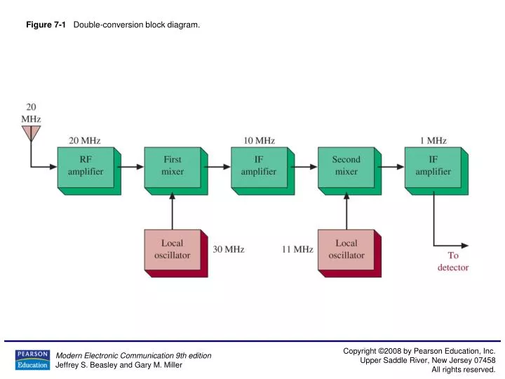
Figure 7-1 Double-conversion block diagram. Figure 7-2 Image frequency rejection. Figure 7-3 System for Example 7-2. Figure 7-4 Up-conversion system. Figure 7-5 AGC characteristics. Figure 7-6 Delayed AGC configuration.

E N D
Figure 7-7 (a) Auxiliary AGC; (b) the Analog Devices AD8369 variable gain amplifier IC;
Figure 7-7 (continued) (a) Auxiliary AGC; (b) the Analog Devices AD8369 variable gain amplifier IC;
Figure 7-11 Third-order intercept and compression point illustration.
Figure 7-12 IMD products (second-, third-, and fifth-order for two test signals).
Figure 7-13 IMD testing: (a) mixer; (b) Class AB linear power amplifier.
Figure 7-18 The Cobra 19 DX IV CB radio. (Courtesy of Cobra Electronics Corporation.)
Figure 7-20 Printed circuit board details: (a) printed circuit layout for CB synthesizer; (b) component layout for CB synthesizer.
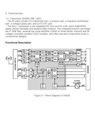
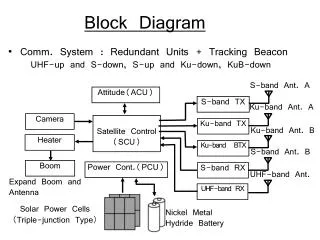
Figure 7-21 UCR110 block diagram. (Courtesy of Lectrosonics, Inc.)
Figure 7-22 The schematic of a UHF multifrequency receiver. (Courtesy of Lectrosonics, Inc.)
Figure 7-25 The ZAS-3 attenuator. (Courtesy of Mini-Circuits: www.minicircuits.com.)
Figure 7-26 The connections for the ZAS-3 attenuator when used as an AM modulator.
Figure 7-27 The suggested biasing for the ZAS-3 control port. (Courtesy of Mini-Circuits: www.minicircuits.com.)
Figure 7-28 The Mini-Circuits ZX95-100 voltage controlled oscillator. (Courtesy of Mini-Circuits: www.minicircuits.com.)
Figure 7-29 The suggested connection diagram for using the ZX95-100 for generating an FM signal. (Courtesy of Mini-Circuits: www.minicircuits.com.)
Figure 7-30 The Mini-Circuits ZP-3 mixer circuit. (Courtesy of Mini-Circuits: www.minicircuits.com.)
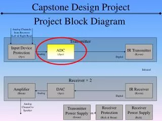
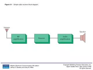
Figure 7-32 Block diagram of a mobile FM transceiver, transmitter portion.
Figure 7-34 The output of the mixer as viewed with an oscilloscope. The input frequencies to the mixer are 20 and 21 MHz.
Figure 7-35 The output of the mixer as viewed by a spectrum analyzer.
Figure 7-36 An example of a squelch circuit as implemented with Multisim.