ASTAR (EBSD-TEM like )
ASTAR (EBSD-TEM like ) Automatic Crystal Orientation/Phase mapping for TEM. www.nanomegas.com. NEW precession application “EBSD” – TEM. EBSD-TEM : beam is scanned over the sample ( eg. 10 m x 10 m )
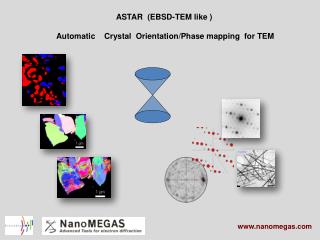

ASTAR (EBSD-TEM like )
E N D
Presentation Transcript
ASTAR (EBSD-TEM like ) Automatic Crystal Orientation/Phase mapping for TEM www.nanomegas.com
NEW precession application “EBSD” – TEM
EBSD-TEM : beam is scanned over the sample ( eg. 10 m x 10 m ) spot electron diffraction patterns are collected ( NOT sensitive to stress/ strain or surface sample preparation like in EBSD-SEM ) Beam scanning performed by “spinning star” unit / no STEM need Thousands of experimental spot ED patterns are acquired by a very fast optical CCD camera attached to TEM screen ( 180 patterns/sec ) Slow scan CCD can also be used ( but slow : 20-30 patterns/sec ) Thousands of theoretical ED patterns are generated ( templates ) from .cif files or commercial databases for all known phases in a sample Template matching is used ( by cross-correlation of all experimental ED patterns with all templates ) to generate most probable orientation of every scanned position in the sample.
1 µm Comparison SEM-(EBSD) vs TEM spatial resolution SEM orientation map deformed Ta6V alloy TEM orientation map (25 nm stepsize) EBSD map (100 nm stepsize) Electron Backscattering Diffraction (EBSD ) orientation maps in SEM have usually poor resolution in comparison with TEM maps showing detailed nanostructure
ASTAR : diffraction pattern adquisition 1 µm Example :Severely deformed 7075 Aluminium Alloy Any TEM –FEG/LaB6 may work with ASTAR
1 µm EBSD-TEM : Automated Crystal Orientation Mapping Kikuchi pattern Orientation W + W’(= W +0.1°) Orientation W Severely deformed 7075 Al. Alloy Bragg Spot pattern
Computer Beam Control Image Processing D.A. Board Camera Frame Grabber ASTAR ( EBSD-TEM Procedure ) Control Phase /orientation maps generation (off-line) Beam scanning Dedicatedprecession unit « Spinning Star » -DigiSTAR ASTAR : Automatic Crystal Orientation and phase mapping hardware /software package for TEM
Dedicated fast CCD camera (> 100 patterns/sec) attached to the TEM screen
DiffGen : Template generator Features: Any crystallographic structure Laue class adapted to the space group Structure generator (space group, structure factor equ.)
ASTAR : crystallographic orientation identification Template generation of all possible simulated orientations (every1º) withinstereographic triangle for givencrystallattice(s) and symmetry Pre-calculated templates 001 101 1-11 111 Correlation index Acquired pattern Stereographic projection (example ,cubic) ~2000 simulated patterns Degree of matching between experimental patterns and simulated templates is given by a correlation index ; highest value corresponds to the adequate orientation/phase
ASTAR : pattern matching by image cross- correlation Correlation index Image treatment Cross-correlation comparison of all acquired ED patterns with all simulated templates to deduce correct pattern index; degree of matching between experimental patterns and simulated templates is given by a correlation index where highest value corresponds to the adequate orientation/phase.
ASTAR identification example : nanocrystalline Cu 111 100 110 correlation index = 585 Diffraction pattern ( nanocrystalline cubic copper) Correlation index map For a given ED pattern, the correlation index map is calculated for all possible template orientations and plotted on a map that represents a portion of the stereographic projection (reduced to a double standard triangle). That resulting map reveals the most probable orientation for every experimental spot ED pattern ( in this case ED pattern is found to be close to 110 ZA orientation )
ASTAR : ultra-fast TEM orientationmap Sample : severelydeformedcopper 250 x 200 pixel data adquisition 5 min !! Typical software data analysis time ( forcubic ) 5-15 min ( hexagonal , tetragonal ) x 3- 4 more time Orientation map NBD step 20 nm
Comparison of TEM image, and ASTAR results 15 nm resolution • CM20 UTwin LaB6 courtresy Prof . S.Godet ULB Brussels 0.5µm
Pt nanoparticles , Cu lines in semiconductors ( FEG –TEM ) Orientation (EBSD-like maps) at 1 nm resolution ! Courtesy Jeol Japan- Jeol 2100F Pt nanoparticles ASTAR phase/orientation TEM device with Jeol 2010 FEG , Jeol 2200 FS ,1 nm spot size NBD mode, 150x150 pixel, step size 1 nm , 15 min adquis. time Courtesy Prof. P.Ferreira , Ganesh Univ Texas at Austin Dr. Holm Kirmse Humboldt Univ Berlin
(Mn ,Ga) As clusters in GaAs matrix Virtual bright field map Orientation map Phase map Reliability map GaAs cubic F-43m (216) a= 0.56533 nm MnAs b phase orthorhombic P21/n21/m21/a (62) a= 0.5704 nm, b= 0.3655 nm, c= 0.6365 nm MnAs a phase hexagonal P63/mmc Courtesy Dr. Ines Haeusler Berlin Humboldt University, Germany
Si (matrix) and SiC b 3C (a= 0.436 nm) Which orientation relation between matrix – precipitates? VBF Reliability Index Orientation map Si cubic a= 0.5428 nm Grain size 100-500 nm Jeol 3010, 25 nm spot size Phase map: Si red, SiC blue Courtesy T Epicier Univ LYON
Orientation (a)and phase map of TiNb alloy revealing cubic phase (in red a= 0.332 nm Im-3m) and orthorhombic phase ( in blue a=0.3215 nm, b=0.485 nm, c=0.462 nm Cmcm ) c d a b Orientation(c) and phase map d) of AlCu alloy (in green AlCu monoclinic phase C2/m a=1.206 nm, b=0.410 nm, c=0.691 nm, b = 54,04º , in red Al3Cu4 orthorhombic phase Fmm2 a= 0.812 nm, b= 1.419, c= 0.999 nm ) courtesy Prof.V.Demange V.Dorcet, Univ Rennes France
INDEX : pattern identification software Diffraction Pattern Block viewer Virtual dark field image
TEMdpa : Virtual Bright Field on-line construction Orientation map Bright field
VBF index reliability VBF reliability index ASTAR (EBSD -TEM) orientation maps : Nanotwins in Cu CBD mode Jeol 3010 microscope
ASTAR : Reliability Superimposed diffraction patterns at a grain bounday Stereographic projection Templates for copper Q2 Q1 Q1> Q2 R = 100 (1- Q2/Q1) Reliability
Deconvolution of superimposed Diffraction patterns Grain 1 Grain 2
Imaging Grain Boundaries Deformed Zr alloy(Zirkaloy 4 rolled down 78%) bright field TEM image (left) showing poor grain boundary contrast, area 5x5 mm (center)same area ASTAR orientation map (right) highlighted grain boundaries with angle > 15º a b c
Courtesy Nippon Steel Additional information obtained during this experiment : Study of Twins Study of Precipitates Identification of the various precipitates : - Cementite (blue) - TiN (red) 100x100 scanned at a rate of 44 fps (23 min). Step size 12 nm
Twin analysisin deformedsteelsamples matrix reflections e f twin reflections Virtual dark field TWIP deformed steel Courtesy Prof. S.Godet Univ Brussels (ULB) Belgium
0º 0.5º 1º As the precession angle increases from 0º to 3º, the diffraction pattern goes to higher resolution (i.e. more diffraction spots are seen). 2º 3º
ASTAR : combine scanning withprecession NO precession precession Using precession diffraction the number of ED spots observed increases ( almost double ) ; correlation index map becomes much more reliable when compared with templates NO precession (Index 622 ) Orientation map INCORRECT orientation In this example (right) a metal particle gives wrong correlation index without precession due to presence of Kikuchi lines; after applying precession (right lower image), index gets correct value as ED quality improves and Kikuchi lines dissapear 0.5° precession (Index 745 ) CORRECT orientation
Mayenite mineral Samecrystaltilted 0-20º 400 patternscollected Precessionangle 0.25º
EBSD-TEM : orientationmapswith and withoutbeamprecession orientationmap, NO precession beamscanningstep 28 nm VBF In thisexamplethreedifferentcubicmayenitecrystalsCa12Al14O33are analyzedwith ASTAR ; orientationmapgeneratedwithoutprecessionresults in inconsistentindexoverareasthatmusthaveuniformorientation. Onthecontrary, orientationmapsgeneratedwithsmallprecessionanglepresent true uniformorientationover individual grains orientationmap precessionangle 0.25º CONCLUSION Orientation maps are more precise with precession
ASTAR : Phasemapswith and withoutprecession 3 existing phases: only possible to distinguish by precession Orientationmap VBF When stacking faults cross themselves, they produce locally a ´ martensite structure (a= 2.87 A) Austenitic matrix with g fcc structure (a=3.58 A) crystalphasemap Stacking faults with e hexagonal structure (a=2.57 c= 4.08 A) NO precession precession 0.4º
EBSD like-TEM : copper lines ( FEG –TEM ) No precession Bright field precession 0.6 deg Jeol 2010 FEG Univ Texas -Austin ,1 nm spot size NBD mode, 200x200 pixel, step size 9 nm Courtesy Prof. P.Ferreira , Ganesh Univ Texas at Austin
Pt nanoparticles ( FEG –TEM ) No precession precession 0.5 deg Jeol 2010 FEG Univ Texas -Austin ,1 nm spot size NBD mode, 150x150 pixel, step size 1 nm recent unpublished results
Nanoparticle ( 50 nm ) phase identification cubic 8.32 A Magnetite or maghemite ?? -Fe2O3 Fe3O4 cubic 8.32 A ALL Nanoparticles REVEALED AS magnetite (RED ) Orientation map precession 0.3º PHASE map precession 0.3º
Grain and phase boundaries: solving 180°ambiguity with precession The ambiguity in the indexing of ED spot patterns arises from the fact that a particular reflection may be indexed either as (hkl) or (-h-k-l). While this ambiguity is irrelevant for some applications, it becomes important for determination of grain and phase boundary parameters. a [103] [-10-3] h [103] Wronglydetected particle (austenite ) True austenite phase ASTAR + precession ASTAR + precession TRIP steel (bcc ferrite + fcc austenite) ; Philips CM120 (6 min scanning ),
Indexing high resolution image of anatase - TiO2 it is possible to detect automatically the nanoparticle orientation: close to [100]
ASTAR : Phase /orientation mapping HREM images • Fast Fourier Transforms are performed on successive subsets of the high resolution image as if the sample was scanned. • The resulting patterns are compared to templates • Orientations and/or phases may be recognized • a small subset leads to higher spatial resolution • - larger subimages improve the indexing quality FFT over 256x256 subimages • TITAN-Cubed : PbSe nanocrystals • Credits: Marie CHEYNET, SIMaP - Grenoble INP • Odile ROBBE, LASIR – UTS Lille Orientation map (color) combined to INDEX (gray scale) Titan Cs corrected HREM : PbSe nanoparticles
Precession adds a value to EBSD-TEM technique : ED patterns acquired with precession contain less dynamical effects , more spots and when compared with templates give much better correlation-reability than ED patterns without precession Correlation index for many reflections highly increases even at small precession angles ( eg 0.2 º -0.5º ) Orientation maps for several materials are of much better quality with precession Phase maps for several materials are of much better quality with precession ( much less artifacts or ambiguities ) In orientation-phase maps “180º ambiguity ” for cubic crystals can be solved using precession
1st precession electron diffraction user meeting Workshop Electron Precession ebsd-tem ICM17 Rio de Janeiro Brazil 22-23 September 2010 Electron Crystallography in Physical and Biological Science (AsCA2010 Satellite Meeting, KBSI, Daejeon) 29-30 October 2010 www.nanomegas.com
TEM ELECTRON DIFFRACTION SOLUTIONS AUTOMATIC ORIENTATION / PHASE MAPPING 3D PRECESSION DIFFRACTION TOMOGRAPHY PRECESSION UNIT « DigiStar » Basic platform ELECTRON DIFFRACTOMETER-