Download
1 / 21
210 likes | 360 Views
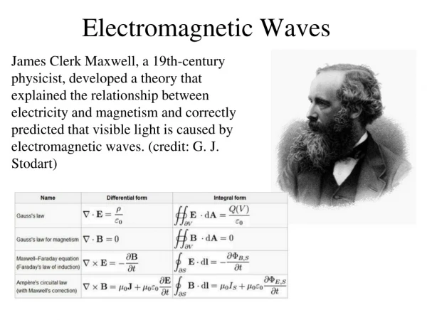
1. Figure 13.1 Electromagnetic waves. 13.1 GALLIUM ARSENIDE VERSUS SILICON. 13.1.1 Dielectric-Semiconductor Interface : Enhancement Versus Depletion FETs. Figure 13.2 Comparison of enhancement-type MOSFET and depletion-type FET. 13.1.3 Electron Mobility and Saturation Velocity.

E N D
Figure 13.1 Electromagnetic waves. Principles of Semiconductor Devices Dimitrijev
13.1 GALLIUM ARSENIDE VERSUS SILICON 13.1.1 Dielectric-Semiconductor Interface : Enhancement Versus Depletion FETs Figure 13.2 Comparison of enhancement-type MOSFET and depletion-type FET. Principles of Semiconductor Devices Dimitrijev
13.1.3 Electron Mobility and Saturation Velocity Figure 13.3 Drift velocity versus electric field in GaAs. Principles of Semiconductor Devices Dimitrijev
13.2 JFET 13.2.1 JFET Structure Figure 13.4 JFET structure. Principles of Semiconductor Devices Dimitrijev
13.2.2 JFET Characteristics Figure 13.5 JFET in triode region. (a) Cross section, (b) energy bands, and (c) point Q showing the bias conditions on ID–VDScharacteristics. Principles of Semiconductor Devices Dimitrijev
Figure 13.6 JFET in the saturation region. (a) Cross section, (b) energy bands, and (c) point Q showing the bias conditions on ID–VDScharacteristics. Principles of Semiconductor Devices Dimitrijev
Figure 13.7 JFET in cutoff region. (a) Cross section, (b) energy bands, and (c) point Q showing the bias conditions on ID–VDScharacteristics. Principles of Semiconductor Devices Dimitrijev
13.2.3 SPICE Model and Parameters Table 13.1 Summary of SPICE JFET Model: The Principal Equivalent-Circuit Elements Principles of Semiconductor Devices Dimitrijev
Table 13.2 Summary of SPICE JFET Model: Parasitic Elements Principles of Semiconductor Devices Dimitrijev
13.3 MESFET 13.3.1 MESFET Structure Figure 13.8 MESFET structure. Principles of Semiconductor Devices Dimitrijev
13.3.2 HEMT Characteristics Figure 13.9Transfer and output characteristic of a MESFET. Principles of Semiconductor Devices Dimitrijev
13.3.3 SPICE Model and Parameters (13.1) (13.2) (13.3) (13.4) Table 13.3 Summary of SPICE MESFET Model Principles of Semiconductor Devices Dimitrijev
13.4 HEMT 13.4.1 Two-Dimensional Electron Gas (2DEG) Figure 13.10 Illustration of energy level quantization that creates two-dimensional electron gas (2DEG). Principles of Semiconductor Devices Dimitrijev
Figure 13.11 Cross section and energy-band diagram of an AlGaAs–GaAs system. Principles of Semiconductor Devices Dimitrijev
13.4.2 HEMT Structure and Characteristics Figure 13.12 HEMT structure and energy bands at source and drain contacts. Principles of Semiconductor Devices Dimitrijev
13.5 NEGATIVE RESISTANCE DIODES 13.5.1 Amplification and Oscillation by Negative Dynamic Resistance (13.5) (13.6) (13.7) (13.8) (13.9) (13.10) Figure 13.13 Signal amplification by a negative-conductance diode. (a) Fundamental small-signal equivalent circuit. (b) Graphic load-line analysis. Principles of Semiconductor Devices Dimitrijev
13.5.2 Gunn Diode Figure 13.15 Illustration of the negative-dynamic conductance/resistance due to the Gunn effect. Principles of Semiconductor Devices Dimitrijev
(13.11) Figure 13.16 Illustration of a Gunn-effect oscillator. Principles of Semiconductor Devices Dimitrijev
13.5.3 IMPATT Diode (13.12) Figure 13.17 The principle of IMPATT diode operation. Principles of Semiconductor Devices Dimitrijev
13.5.4 Tunnel Diode Figure 13.18 The principle of tunnel diode operation. Principles of Semiconductor Devices Dimitrijev