Download
1 / 40
460 likes | 637 Views
Explore the detailed steps of CMOS fabrication on a silicon wafer, including lithography, inverter cross-section, mask sets, and key fabrication steps like n-well formation and metallization. Learn about design rules, stick diagrams, and the challenges faced in the manufacturing process.

E N D
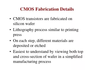
CMOS Fabrication Details • CMOS transistors are fabricated on silicon wafer • Lithography process similar to printing press • On each step, different materials are deposited or etched • Easiest to understand by viewing both top and cross-section of wafer in a simplified manufacturing process
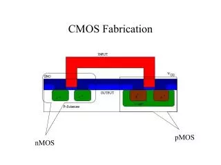
Inverter Cross-section • Typically use p-type substrate for nMOS transistors • Requires n-well for body of pMOS transistors
Well and Substrate Taps • Substrate must be tied to GND and n-well to VDD • Metal to lightly-doped semiconductor forms poor connection called Shottky Diode • Use heavily doped well and substrate contacts / taps
Inverter Mask Set • Transistors and wires are defined by masks • Cross-section taken along dashed line
Detailed Mask Views • Six masks • n-well • Polysilicon • n+ diffusion • p+ diffusion • Contact • Metal
Fabrication Steps • Start with blank wafer • Build inverter from the bottom up • First step will be to form the n-well • Cover wafer with protective layer of SiO2 (oxide) • Remove layer where n-well should be built • Implant or diffuse n dopants into exposed wafer • Strip off SiO2
Oxidation • Grow SiO2 on top of Si wafer • 900 – 1200 C with H2O or O2 in oxidation furnace
Photoresist • Spin on photoresist • Photoresist is a light-sensitive organic polymer • Softens where exposed to light
Lithography • Expose photoresist through n-well mask • Strip off exposed photoresist
Etch • Etch oxide with hydrofluoric acid (HF) • Seeps through skin and eats bone; nasty stuff!!! • Only attacks oxide where resist has been exposed
Strip Photoresist • Strip off remaining photoresist • Use mixture of acids called piranah etch • Necessary so resist doesn’t melt in next step
n-well • n-well is formed with diffusion or ion implantation • Diffusion • Place wafer in furnace with arsenic gas • Heat until As atoms diffuse into exposed Si • Ion Implanatation • Blast wafer with beam of As ions • Ions blocked by SiO2, only enter exposed Si
Strip Oxide • Strip off the remaining oxide using HF • Back to bare wafer with n-well • Subsequent steps involve similar series of steps
Polysilicon • Deposit very thin layer of gate oxide • < 20 Å (6-7 atomic layers) • Chemical Vapor Deposition (CVD) of silicon layer • Place wafer in furnace with Silane gas (SiH4) • Forms many small crystals called polysilicon • Heavily doped to be good conductor
Polysilicon Patterning • Use same lithography process to pattern polysilicon
Self-Aligned Process • Use oxide and masking to expose where n+ dopants should be diffused or implanted • N-diffusion forms nMOS source, drain, and n-well contact
N-diffusion • Pattern oxide and form n+ regions • Self-aligned process where gate blocks diffusion • Polysilicon is better than metal for self-aligned gates because it doesn’t melt during later processing
N-diffusion cont. • Historically dopants were diffused • Usually ion implantation today • But regions are still called diffusion
N-diffusion cont. • Strip off oxide to complete patterning step
P-Diffusion • Similar set of steps form p+ diffusion regions for pMOS source and drain and substrate contact
Contacts • Now we need to wire together the devices • Cover chip with thick field oxide • Etch oxide where contact cuts are needed
Metallization • Sputter on aluminum over whole wafer • Pattern to remove excess metal, leaving wires
Stick Diagrams VLSI design aims to translate circuit concepts onto silicon stick diagrams are a means of capturing topography and layer information - simple diagrams Stick diagrams convey layer information through colour codes (or monochrome encoding Used by CAD packages, including Microwind
Design Rules • Allow translation of circuits (usually in stick diagram or symbolic form) into actual geometry in silicon • Interface between circuit designer and fabrication engineer • Compromise • designer - tighter, smaller • fabricator - controllable, reproducable
Lambda Based Design Rules • Design rules based on single parameter, λ • Simple for the designer • Wide acceptance • Provide feature size independent way of setting out mask • If design rules are obeyed, masks will produce working circuits • Minimum feature size is defined as 2 λ • Used to preserve topological features on a chip • Prevents shorting, opens, contacts from slipping out of area to be contacted
Design Rules - The Reality • Manufacturing processes have inherent limitations in accuracy and repeatability • Design rules specify geometry of masks that provide reasonable yield • Design rules are determined by experience
Problems - Manufacturing • Photoresist shrinking / tearing • Variations in material deposition • Variations in temperature • Variations in oxide thickness • Impurities • Variations between lots • Variations across the wafer
Problems - Manufacturing • Variations in threshold voltage • oxide thickness • ion implantation • poly variations • Diffusion - changes in doping (variation in R, C) • Poly, metal variations in height and width -> variation in R, C • Shorts and opens • Via may not be cut all the way through • Undersize via has too much resistance • Oversize via may short
Meta Design Rules • Basic reasons for design rules • Rules that generate design rules • Under worst case misalignment and maximum edge movement of any feature, no serious performance degradation should occur
Advantages of Generalised Design Rules • Ease of learning because they are scalable, portable, durable • Longlevity of designs that are simple, abstract and minimal clutter • Increased designer efficiency • Automatic translation to final layout
Basic Interconnects • Wiring-Up of chip devices takes place through various conductors produced during processing • Today, interconnects constitute the main source of delay in MOS circuits • We will examine: • Sheet Resistance – Resistance / Unit Area • Area Capacitance • Delay Units • CMOS Inverter Delay • Rise and Fall Time Estimation
Sheet Resistance • Resistance of a square slab of material • RAB = ρL/A t • => R = ρL/t*W • Let L = W (square slab) • => RAB = ρ/t = Rs ohm / square A t L w B RAB = ZRsh Z = L/W
Typical sheet resistance values for materials are very well characterised Typical Sheet Resistances for 5µm Technology
N-type Minimum Feature Device Polysilicon L N - diffusion 2λ W 2λ R = 1sq x Rs = Rs = 104 Ώ
Area Capacitance of Layers • Conducting layers are separated from each other by insulators (typically SiO2) • This may constitute a parallel plate capacitor, C = є0єox A / D (farads) • D = thickness of oxide, A = area, • єox = 4 F/µm2 • Area capacitance given in pF/µm2
Capacitance • Standard unit for a technology node is the gate - channel capacitance of the minimum sized transistor (2λ x 2λ), given as Cg • This is a ‘technology specific’ value
Delay Unit • For a feature size square gate, τ = Rs x Cg • i.e for 5µm technology, τ = 104 ohm/sq x 0.01pF = 0.1ns • Because of effects of parasitics which we have not considered in our model, delay is typically of the order of 0.2 - 0.3 ns • Note that τ is very similar to channel transit time τsd
Inverter Layout • Transistor dimensions specified as Width / Length • Minimum size is 4l / 2l, sometimes called 1 unit • In f = 0.6 mm process, this is 1.2 mm wide, 0.6 mm long