Download
1 / 23
230 likes | 364 Views
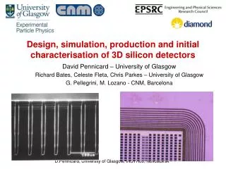
Technology of p-type microstrip detectors with radiation hard p-spray, p-stop and moderate p-spray insulations. G.Pellegrini 1 , C.Fleta 2 , F.Campabadal 1 , M. Lozano 1 , J.M. Rafí 1 , M.Ullán 1 1 Centro Nacional de Microelectr ó nica, Barcelona Spain 2 University of Glasgow, Glasgow, UK.

E N D
Technology of p-type microstrip detectors with radiation hard p-spray, p-stop and moderate p-spray insulations G.Pellegrini1, C.Fleta2, F.Campabadal1, M. Lozano1, J.M. Rafí1, M.Ullán1 1Centro Nacional de Microelectrónica, Barcelona Spain 2University of Glasgow, Glasgow, UK
Outline • P-type detectors • Detector isolation technologies • Simulation and measurements • Conclusions
Technology: N type strips on p-type substrate N side read-out takes advantage of the presence of the high electric field on the read-out side after irradiation. Needs insulation between strips in order to compensate the electron layer formed below the oxide: P-stop P-spray Moderate p-spray More complex technology 6 or 7 photolithographic layers The most radiation hard technology P-type detectors
First n-on-p detectors fabricated with p-stop isolation. Different implants were used to find the optimum value. P-stop isolation Pitch 120mm, p-stop width 7mm, strip width 20mm
Radiation hardness N-on-p strip detectors with p-stop isolation (1) Pad detectors (2) • Baby microstrip detectors fabricated at CNM in collaboration with Liverpool University Efficiency of Charge Collection in 280 um thick p-type SSD After 7.5 *1015 p/cm2, charge collected is > 6,500 e- • First results on charge collection efficiency of heavily irradiated microstrip sensors fabricated on oxygenated p-type silicon. NIM-A, num 518, Feb. 2004, pp. 340-342. G. Casse, P.P. Allport, S. Martí, M. Lozano, P. R. Turner. • Comparison of radiation hardness of P-in-N, N-in-N and N-in-P silicon pad detectors IEEE Trans. on Nucl. Sci., V. 52, Issue 5, Part 2, Oct. 2005 Page(s):1468 – 1473, M. Lozano, G. Pellegrini, C. Fleta, C. Loderer, J. M. Rafí, M. Ullán, F. Campabadal, C. Martínez, M. Key, G. Casse, P. Allport
Annealing p-type Annealing (@80 oC) behaviors of the collected charge after proton irradiation to 3.5. 1015 cm-2. At high voltage the collected charge appears to be stable. It is known that the full depletion voltage as determined by CV measurements appears to follow the expected evolution. Pad detectors N-on-p strip detectors with p-stop isolation G. Casse, “Overview of n-side read-out microstrip devices”, RD50/FDS meeting 2005. “Annealing Studies of Magnetic Czochralski Silicon Radiation Detectors”, G.Pellegrini et al., Nucl. Instr. and Meth. Volume 552, Issues 1-2, 21 October 2005.
Electronic Noise micro-discharge noise Micro-discharges can represent the earliest mechanism of failure for micro-strip detectors when operated at high voltage. Baby microstrip detectors fabricated by Hamamatsu G. Casse, “Overview of n-side read-out microstrip devices”, RD50/FDS meeting 2005.
To avoid the problem of microdischarges p-spray isolation was used to fabricate microstrip and pad detectors. P-spray isolation • P-spray has to: • Insulate strips • Keep VBD > VFD • Variables: • Oxide thickness • Implant dose • Implant energy • Thermal budget fixed • Optimization through: • Simulation (ISE-TCAD) • Engineering runs (3) Conflicting conditions
Simulation of p-spray Electric field at the breakdown point
P-spray: calibration runs Characteristics of n-in-p pad detectors with p-spray isolation
Effect of oxidecharge • Fast build-up of damage in the oxide layer • Reach a saturation value for the oxide charge of about 2-31012 cm-2 at about 100-200 krad (few LHC weeks) • The oxide charge will be saturated well before the bulk damage will start to affect the operation of the detectors • This oxide charge increases inversion layer, canceling the p-spray insulation • It is very important to ensure that insulation is maintained after first irradiation, not only in fresh or bulk damaged detectors. • Irradiation: • 50 Mrad, • Co60 gamma source • MOS Capacitor CV measurements • Oxide charge • Before: 11011 cm-2 • After: 31012 cm-2 “Technology development of p-type microstrip detectors with radiation hard p-spray isolation” , G. Pellegrini et al., Nucl. Instr. and Meth A 2006 In Press, Corrected Proof, Available online 28 July 2006 Strip detector
Neutron irradiation Signal induced by 1060 nm pulsed laser illumination, n-in-p detector after 7.5 1015 p cm-2. (G.Casse,RD50 Status Report 2004) P-type irradiated with neutrons (1015 n/cm2) • read a 3cm p-type detector using the ATLAS SCTDAC readout. • SCTDAC is optimised for n-type sensor. • SCT readout: binary ABCD3T chip Please look at C. Lacasta poster in this conference
Final process Rd50 mask Guard rings CCE and noise measurements on strip detector undergoing by RD50 collaboration
P-spray vs p-stop • P-spray • Is a critical technology • Low repeatability of the p-spray process. • Detectors performance are very sensitive to the p-spray isolation dose implanted. • Isolation dependent on charge oxide before and after irradiation • The surface damage usually leads to higher leakage currents before irradiation • P-stop • Requires a minimum strip pitch depending on the design rules of the manufacturer • ‘Leaky channels’ can severely reduce the yield, hence the necessity of a minimum width of the p-stop implant • High electrical field in P-stop corner • This high electric files may cause micro-discharge noise
Moderated p-spray • We can take the best from the two options: Moderated P-spray • An old (1997) patent from MPI presented the basics • Technology has to be optimized • We have developed through simulation a technology for p-type detectors with moderated p-spray insulation • Boron implant parameters are selected from our previous experience with microstrip with p-stops • With less p-spray implanted charge, we obtain: • Higher breakdown voltages • Good insulation before and after irradiation • Eliminate the high field corner in the p-stop causing microdischarges • No necessity of redundancy in the p-stop implants.
Simulated device RD50 mask set (pitch 80 μm, strip width 32 μm) Single p-stop between the strips: width 10 μm Substrate: P-type, <100>, 30 kΩ·cm Oxide charge density: 1011 cm-2 (non-irradiated device) P-implant parameters: Fixed energy, dose: 50 keV, 1013 cm-2 Fixed oxide implant thickness for the p-stop area We have fabricated devices with these p-stop implant parameters and they show a satisfactory electrical behavior The objective of the simulations is to determine the optimum profile in the p-spray area Simulation of moderated p-spray
First: oxidation, photolithography p-stop regions, wet oxide etching, oxidation, photoresist striping At this point there are two different oxide thicknesses thin oxide in the p-stop area and a thicker oxide on the rest of the silicon surface (“p-spray area”) P-implant (Energy 50 keV, dose 1013 cm-2) Finish with the usual fabrication process Technology
Simulated Devices profiles I-V curves
Doping profile comparison N strip P-stop P-stop only P-spray Moderated p-spray
Electric field comparison N strip microdischarches? P-stop P-stop only P-spray Moderated p-spray
Experimental Results Test structure to measure interstrip resistance
P-type detectors seems the best detector option for the future sLHC experiments as they gather beneficial properties: electron collection junction always at the strip side partial depletion operation possible very high radiation hardness stable annealing We have developed three technologies for p-type detectors with the different isolation techniques: p-spray, p-stops and moderated p-spray Detectors have been fabricated, irradiated with protons, neutrons, and gammas, and they work properly Conclusions