Download
1 / 8
80 likes | 101 Views
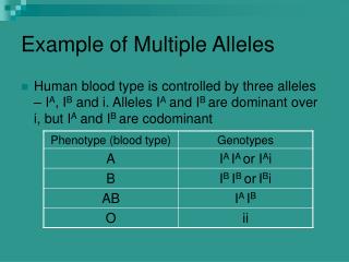
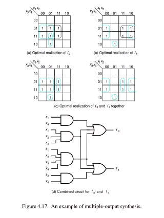
This article discusses the optimal realization of two functions, f and f, in a combined circuit. It includes examples of multiple-output synthesis and conversion to NOR-gate and NAND-gate circuits.

E N D
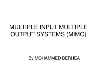
x x x x 1 2 1 2 x x x x 3 4 3 4 00 01 11 10 00 01 11 10 00 00 01 1 1 1 01 1 1 1 11 1 1 1 11 1 1 1 10 1 10 1 (a) Optimal realization of (b) Optimal realization of f f 3 4 x x x x 1 2 1 2 x x x x 3 4 3 4 00 01 11 10 00 01 11 10 00 00 01 1 1 1 01 1 1 1 11 1 1 1 11 1 1 1 10 1 10 1 (c) Optimal realization of f and f together 3 4 x 1 x 4 x f 1 3 x 2 x 4 x 1 x 2 x 3 x f 4 4 x 2 x 4 f f (d) Combined circuit for and 3 4 Figure 4.17. An example of multiple-output synthesis.
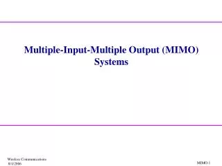
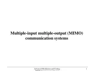
x x x x 1 2 1 2 x x x x 3 4 3 4 00 01 11 10 00 01 11 10 00 1 00 01 1 1 1 01 1 1 1 1 11 1 11 1 1 1 1 10 1 1 1 10 x = 0 x = 1 5 5 (a) Karnaugh map for the function f x 1 g x 2 x 5 x f 3 k x 4 (b) Circuit obtained using decomposition Figure 4.25. Conversion to a NOR-gate circuit.
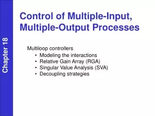
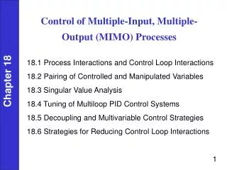
x 1 x 2 x 3 f x 4 x 5 x 6 x 7 (a) Circuit with AND and OR gates x 1 x 2 x 3 x f 4 x 5 x 6 x 7 (b) Inversions needed to convert to NANDs x 1 x 2 x 3 x f 4 x 5 x 6 x 7 Figure 4.27. Conversion to a NAND-gate circuit.
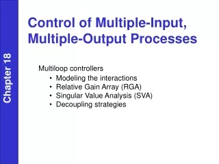
x 1 x 2 x 3 f x 4 x 5 x 6 x 7 (a) Inversions needed to convert to NORs x 1 x 2 x 3 f x 4 x 5 x 6 x 7 Figure 4.28. Conversion to a NOR-gate circuit.
Prime Minterm implicant 0 2 5 6 7 8 9 13 p 0 0 x 0 1 p 0 x 1 0 2 p 0 1 1 x 3 p x 0 0 x 4 p x x 0 1 5 p 1 x 0 x 6 p x 1 x 1 7 (a) Initial prime implicant cover table Prime Minterm implicant 0 2 5 6 7 8 p 0 0 x 0 1 p 0 x 1 0 2 p 0 1 1 x 3 p x 0 0 x 4 p x x 0 1 5 p 1 x 0 x 6 p x 1 x 1 7 (b) After the removal of columns 9 and 13 Prime Minterm implicant 0 2 5 6 7 8 Prime Minterm implicant 2 6 p 1 p p 2 1 p p 2 3 p p 3 4 p 7 p p (d) After including and 4 7 p p (c) After the removal of rows and in the cover 5 6 Figure 4.39. Selection of a cover.
Figure 4.40. Selection of a cover for the function in Figure 4.15.
Design conception Design entry, initial synthesis, and functional simulation (see section 2.9) Logic synthesis/optimization Physical design Timing simulation No Design correct? Yes Chip configuration Figure 4.48. A complete CAD system.