Download
1 / 1
10 likes | 167 Views
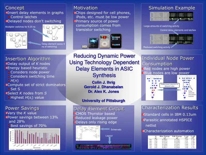
Concept Insert delay elements in graphs Control latches Delayed nodes don’t switching. Simulation Example. Motivation Chips designed for cell phones, iPods, etc. must be low power Primary source of power consumption comes from transistor switching.

E N D
Concept • Insert delay elements in graphs • Control latches • Delayed nodes don’t switching Simulation Example Motivation • Chips designed for cell phones, • iPods, etc. must be low power • Primary source of power • consumption comes from • transistor switching Large amounts of switching activity Multiplier switches for 9.25 ns Control delay elements and latches Delay element saves 5 ns of switching Reduced switching activity Reducing Dynamic Power Using Technology Dependent Delay Elements in ASIC Synthesis Insertion Algorithm • Delay output of K nodes • Energy based heuristic • Considers node power • Considers switching time • H(n) • Compute set of strict dominators • Set S • Select K nodes from S • Highest H(si) value Individual Node Power Consumption • Red nodes are high power • Blue nodes are low power Colin J. Ihrig Gerold J. Dhanabalan Dr. Alex K. Jones University of Pittsburgh Visible power reduction for delayed nodes Delay elements and latches inserted Delay Element Circuit • CMOS Thyristor based • Reduced leakage power • Delays only rising edge Characterization Results • Standard cells in IBM 0.13um • Parasitic annotated HSPICE • netlist • Characterization automation Power Savings • Vary the K value • Power savings between 13% • and 28% • Best savings of 70% Schematic Layout