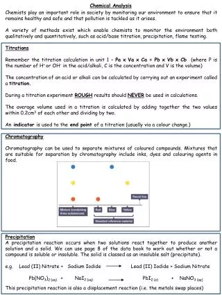
Download
1 / 33
330 likes | 581 Views
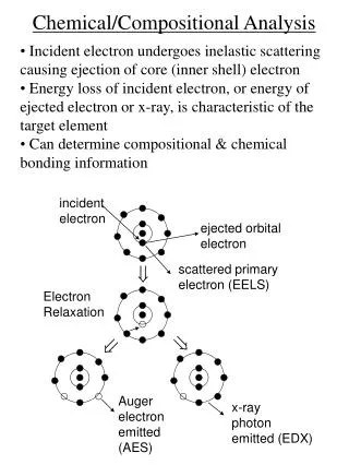
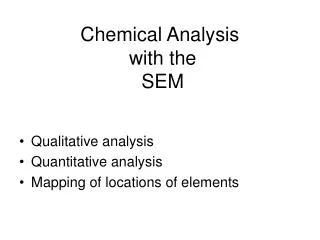
Chemical Analysis with the SEM. Qualitative analysis Quantitative analysis Mapping of locations of elements. Surface Emissions. Pole Piece, etc. SE3. X-rays Cathodoluminescence Photons!. ≈ 1 nm for metals up to 10 nm for insulators. Specimen current. …a little more accurately.

E N D
Chemical Analysis with the SEM • Qualitative analysis • Quantitative analysis • Mapping of locations of elements
Surface Emissions Pole Piece, etc SE3 X-rays Cathodoluminescence Photons! • ≈ 1 nm for metals up to 10 nm for insulators Specimen current
…a little more accurately Shamelessly stolen from Northern Arizona University Microprobe Lab
X-ray generation from inner shell transitions Emission energy is “characteristic” of energy level differences and hence element SEM electron (e.g. 20 keV) “kicks out” electron from “K-shell”
“Kinds of X-rays” • “Characteristic X-rays” • Characteristic of element from which they are emitted • Nominally sharp lines • Brehmstrahlungen • Broad, featureless background • Sanity check: must asymptote to zero at Duane-Hunt limit • Otherwise: evidence of charging!
Characteristic x-rays Brehmstrahlung (baseline/background) X-ray spectrum of sapphire
Fluorescence yield • Fluorescence yield • ωK = K-shell photons emitter per K-shell ionization • For each shell: ωK > ωL > ωM • For Z < 20, the yield drops like a stone! • For carbon, Z=6, ωK ≈ 0.005; for zinc, Z = 30, ωK ≈ 0.5 • Quantitation simply by looking at peak heights, or even areas, is a disaster!
Kinds of X-ray analyzers • Energy dispersive (EDS) • Operate just like a solar cell! • Charge generated by one X-ray: X-ray energy divided by band gap of silicon…well, not really • Wavelength dispersive (WDS) • Bent LiF crystal acts like a conventional glass lens • Degree of deviation in bent crystal depends on X-ray wavelength
X-ray detector “Energy Collection Efficiency” Glenn F. Knoll, Radiation Detection and Measurement, Wiley (1979) p. 503
X-ray detector “Energy Collection Efficiency” Value increases to 3.8 eV at 77 K n.b.!! 1.17 @ 77K Glenn F Knoll, Radiation Detection and Measurement, Wiley (1979)
X-ray analyzer “failure modes” • X-rays from heavier elements (higher energy) can ionize silicon • “Escape peaks” are at energy lower than major peaks by 1.74 keV • Some energy of incident X-ray was used to ionize silicon in detector • Sum peaks • Two X-rays enter detector while counting window is open • Small peak whose energy is the sum of two lower energy peaks.
Sum peak! Aluminum at 1.48 keV Sum peak at 1.98 keV
Spatial Resolution K-O Monte Carlo calculations presumably done for some intermediate Z element Stolen from Goldstein’s lecture
Lab Lecture: How to Actually use the EDAX EDS system • Main software has three tabs: • Spectrum shows only the spectrum • What is a spectrum? • Image • Shows SEM image of area being analyzed • Shows X-ray spectrum • Shows quantitative analysis or histogram of brightness • Mapping • Allows selection of elements to be mapped • Shows spatial distribution of elements in sample
Setting up the NovaNano • Be sure the CCD camera (quadrant) is deselected/not active • Lower the EDS detector to 36 mm • Raise the spot size to 5 or 6 • In the mode setup, choose “EDX mode” • Boot the Genesis software on the support computer (left monitor)
Important tabs on the Genesis window • EDS is an attachment to the SEM • Both Quanta and NovaNano have EDAX systems • Leo has ancient Oxford system. • Genesis is EDAX trade name for EDS operating system
Spectrum tab Mapping tab Image tab
Important icons in Genesis Expand/compress Spectrum horizontally Add text Import spectrum Start/Stop EDS collection Clear spectrum
Genesis icons continued Home: Restore Horizontal and vertical scales Export to Word Expand/compress scale vertically
Preset options What kind of time? Live? Clock? RoI? Determines “Live Time” during which data are collected “None” is also an option
Dead time • Kinds of time • Live time: time during which detector takes data • Dead time: time during which current accumulation window is closed • Clock time • Sum of live and dead time • Actual time we all know and love
Amp time: adjust for dead time of 20 - 40% 1.6 μsec – 102.4 μsec
Microscope control panel and return! Return to normal operating screen
Peak ID Labels from spectrum Halographic Peak Determination: fits spectrum with theoretical sum Possible matches for energy where cursor is located Move to list of labeled peaks
Lower tray information Red while taking data Black when finished
Image Tab You’re image here! Image Tab
Top Center Icons Raster Full Reduced Spot User drawn Return control to microscope!
Brightness and contrast adjust in counterintuitive direction Use low resolution and few strips for faster feedback.