Download
1 / 12
120 likes | 276 Views
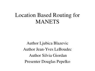
Routing for Reliability in Molecular Diode-based Programmable Nanofabrics. Kushal Datta, Arindam Mukherjee and Arun Ravindran Department of Electrical and Computer Engineering University of North Carolina at Charlotte. MAPLD 2005/1031. Switch Block. Nanofabric Architecture.

E N D
Routing for Reliability in Molecular Diode-based Programmable Nanofabrics Kushal Datta, Arindam Mukherjee and Arun Ravindran Department of Electrical and Computer Engineering University of North Carolina at Charlotte 1 MAPLD 2005/1031
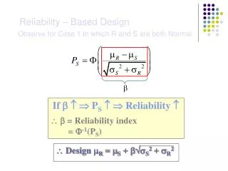
Switch Block Nanofabric Architecture CMOS on Molecular: CMOL Nano Block Diode-based CMU Architecture NanoFabrics: Spatial Computing Using Molecular Electronics Seth Copen Goldstein and Mihai Budiu Proc. of The 28th Annual International Symposium on Computer Architecture, June 2001. 2 MAPLD 2005/1031
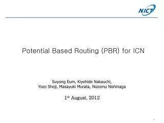
Circuit Primitives Vdd A B f f A B A B f = A . B f = A . B f f = A+B 3 MAPLD 2005/1031
Circuit Primitives Vdd f A B f = A+B Vdd A A A A 4 MAPLD 2005/1031
Nano Electronic Design AutomationAn example Problem Formulation • Given • A logic design • A nanofabric • Constraints • Entry and exit directions of signals in nano/switch blocks • Size of nano and switch blocks • Minimize • The total number of diodes and switches used • Improve robustness 5 MAPLD 2005/1031
Nano EDA Flow VHDL Code Map FPGA Nanofabric PKS + script Placed Nanofabric Boolean Function net list Routing Space Search Flow Map Alternate Routes Decomposed List Our IP optimizer VPACK Optimized Nano Layout Packed List VPR Placed Gate Array 6 MAPLD 2005/1031
Placement • Use a standard algorithm of VPR and get a placed file. • Modify the placed file. • Modification of the placed file involves considering all the possible 12 transformations and deriving equations for them. • Implement a mapping program for this. 7 MAPLD 2005/1031
Placement Sample placed file Equations based on the transformation from the placed file for gate array to the placed file for the nano fabric: x = 2x – z y = 2y – z y B D 0 0 Slice number (z) A C 1 1 F 0 H 0 E G 1 1 x 8 MAPLD 2005/1031
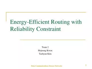
Global Routing Problem Formulation Required AND gate literals enter from West(W) side Required OR gate literals enter from North(N) side If (R (li) = W) & (E (li)=N) 1 extra diode If (R (li) = N) & (E (li)=W) 1 extra diode Vdd li li li li 9 MAPLD 2005/1031
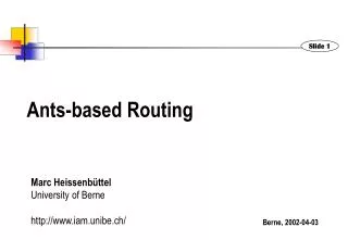
Problem Formulation S1 A l3 l2 l1 S2 B C 10 MAPLD 2005/1031
Future Design Flow VHDL Code Map FPGA Nanofabric PKS + script Placed Nanofabric Boolean Function net list Routing Space Search Flow Map Alternate Routes Decomposed List Our IP optimizer VPACK Optimized Nano Layout Packed List VPR • VLSI-inspired Nano-EDA • Bio-inspired Nano-EDA • High Fault Tolerance • Low Power Placed Gate Array 11 MAPLD 2005/1031
Integrate Placement with Global and Detailed Routing -Improve Fault Tolerance • Simulated Annealing • Moves : • Select switch and nano blocks for placement • Select switch and nano blocks for global routing • Select entry and exit edges for global routing • Select exact entry and exit row/column in a block fro detailed routing 12 MAPLD 2005/1031