Download
1 / 31
310 likes | 334 Views
Learn the basics of BJT amplifier operations, including biasing, linear amplification, AC load lines, and transistor model circuits. Explore common-emitter amplifier configurations and AC analysis techniques.

E N D
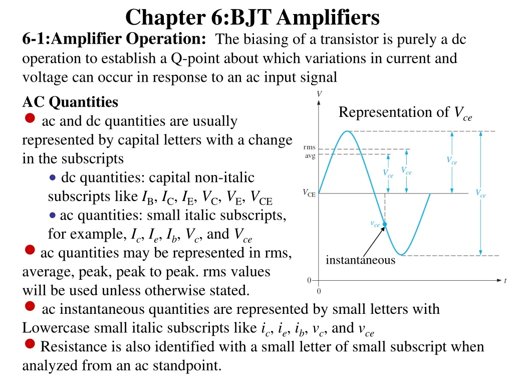
Chapter 6:BJT Amplifiers Representation of Vce instantaneous 6-1:Amplifier Operation: The biasing of a transistor is purely a dc operation to establish a Q-point about which variations in current and voltage can occur in response to an ac input signal AC Quantities • ac and dc quantities are usually represented by capital letters with a change in the subscripts • dc quantities: capital non-italic subscripts like IB, IC, IE, VC, VE, VCE • ac quantities: small italic subscripts, for example, Ic, Ie, Ib, Vc, and Vce • ac quantities may be represented in rms, average, peak, peak to peak. rms values will be used unless otherwise stated. • ac instantaneous quantities are represented by small letters with Lowercase small italic subscripts like ic, ie, ib, vc, and vce • Resistance is also identified with a small letter of small subscript when analyzed from an ac standpoint.
6-1:Amplifier Operation: The linear amplifier • A linear amplifier provides amplification of a signal without any distortion output signal is an exact amplified replica of the input signal. ac source of internal resistance Rs coupled to the base through C1 Load resistance RL coupled to the collector through C2 • The coupling capacitors block dc and thus prevent Rs and RL from changing the dc bias voltages at the base and collector. • For the amplifier shown, notice that the voltage waveform is inverted between the input Vband output Vce but has the same shape.
6-1:Amplifier Operation: AC Load Line • Operation of the linear amplifier can be illustrated using an ac load line as shown. • The ac load line is different than the dc load line because a capacitor looks open to dc but effectively acts as a short to ac the collector resistor RC appears to be in parallel with the load resistor RL.
6-1:Amplifier Operation: Example: a) Determine the resulting peak-to-peak values of collector current and collector-to-emitter voltage from the graph. b) What are the dc Q-point values a) collector current varying from 4 mA to 6 mA collector current has peak-to-peak value of 2 mA (Ic = 2 mA) And Vce = 1 V b) IBQ = 50 μA ICQ = 5mA VCEQ = 1.5V
6-2: Transistor AC Models: • A transistor in an amplifier circuit can be represent by a model circuit. The transistor model circuit based on various internal transistor resistance parameters r that can represent its operation. • Five resistance parameters (r-parameters) can be used for detailed analysis of a BJT circuit. For most analysis work, the simplified r-parameters give good results.
Hence for simplified r-parameter, we have only to be used. can be derived assuming an abrupt p-n junctions 6-2: Transistor AC Models: r-Parameter Transistor Model Simplified to At 20 °C
Determining by a Formula • For the simplified r-parameter, we have only to be considered. can be derived assuming an abrupt p-n junctions • Example: Determine the of a transistor that is operating with a dc emitter current of 2 mA. 6-2: Transistor AC Models: At 20 °C
6-3: The Common-Emitter Amplifier • In the common-emitter (CE) amplifier, the input signal is applied to the base and the inverted output is taken from the collector. The emitter or ground is common to ac signals (Vin and Vout) as shown. CE amplifiers has high voltage gain and high current gain. A common-emitter amplifier with voltage-divider bias and coupling capacitors C1 and C3 on the input and output and a bypass capacitor, C2, from emitter to ground. Output voltage has a 180° phase difference from input voltage.
6-3: The Common-Emitter Amplifier DC analysis • Considering CE amplifier circuit above, dc analysis can be done by removing the coupling and bypass capacitors. Capacitors appear open with dc connected only we will have the voltage divider bias circuit shown. • Using thevenin equivalent for bias circuit (see Ch. 5) RIN(base) > 10 R2 stiff voltage divider
6-3: The Common-Emitter Amplifier AC analysis • Ac equivalent circuit can be developed by considering: • 1- The capacitors are replaced by effective shorts because their values • are selected so that the capacitive resistance XCis negligible at the signal frequency and can be considered to be 0 Ω. • * Note that C2 must be large enough so that XC2 • is very small compared to RE ( ) • At given frequency. XC can be calculated using the relation • 2- The dc source is replaced by ground. No ac voltage can be developed across it so itappears as an ac short. This is why a dc source is called an ac ground. the ac equivalent circuit for CE amplifier is
6-3: The Common-Emitter Amplifier AC analysis: input and output resistances • the total input resistance for voltage divider bias circuit for the input ac voltage is Where Rin(base) for ac is also Rs is series with Rin(tot) • the output resistance for voltage divider bias circuit is the resistance looking in at the collector Hence when RL is capacitively coupled with the circuit, The total output resistance (ac resistance Rc seen by the collector) is RC||RL
6-3: The Common-Emitter Amplifier AC analysis: Voltage gain • ac equivalent circuit for the bias circuit capacitively coupled with RL is With no load, the voltage gain for ac voltage is (see Ch. 4) If C2 is removed
6-3: The Common-Emitter Amplifier AC analysis: Voltage gain • With load resistance RL ac resistance seen by the collector is Rc=RC||RL If C2 is removed To get the overall gain of the amplifier from the source voltage to collector, the attenuation (reduction in signal voltage) of the input circuit must be included. The overall voltage gain of the amplifier Reciprocal of the attenuation
6-3: The Common-Emitter Amplifier AC analysis: Example: for the amplifier shown below, calculate (a) the signal voltage at the base (Vb), (b) the minimum value for the emitter bypass capacitor, C2, if the amplifier must operate over a frequency range from 200 Hz to 10 kHz., (c) Calculate the base-to-collector voltage gain of the amplifier (without and with C2) if there is no load resistor, (d) If a load resistor of 5kΩ is added at Vout, calculate the voltage gain (include C2), and (e) the overall voltage gain if C2 and RL are included (e) the signal voltage at the collector
6-3: The Common-Emitter Amplifier AC analysis: Example – continued. The Ac equivalent circuit of above circuit is shown in the figure below (a) From above dc analysis IE = 3.8 mA hence (b) The XCof the bypass capacitor, C2, should be at least ten times less than RE.
6-3: The Common-Emitter Amplifier AC analysis: Example – continued from previous (c) Without C2 With C2 With RL and C2 included (d) (e) The overall voltage gain is (C2 and RL are included) (f) The signal voltage at the collector Vc
AC analysis: Addition of Swamping Resistor. voltage gain is essentially depends on specially when RE is bypassed by C2. Since changes with temperature the voltage gain becomes unstable. On the other hand, removing C2 cause the gain to go to its lowest value. Hence we can add a swamping resistor (RE1) to reduce the effect of and If = 20 Ω for the transistor 6-3: The Common-Emitter Amplifier Greater gain stability can be achieved and the gain will be lower as a result. The voltage gain for the circuit shown becomes: (if RE1 > 10 ) READ CAREFULLY EXAMPLE 6-8 page 272
6-3: The Common-Emitter Amplifier AC analysis: current gain where AC analysis: power gain Ex. In the example before, calculate the overall current gain and power gain Current gain Power gain
6-4: The Common-collector Amplifier • The common-collector (CC) amplifier is usually referred to as an emitter-follower (EF). The input is applied to the base through a coupling capacitor, and the output is at the emitter (no phase change between input and output). The voltage gain of a CC amplifier is approximately 1, and its main advantages are its high input resistance and current gain. The high input resistance is very useful to minimize the loading effect specially when circuit is driving a low-resistance load CC amplifier is used as a Buffer.
6-4: The Common-collector Amplifier Voltage Gain • The voltage gain is usually can be calculated with the help of ac equivalent for input and output voltage shown. and Therefore the voltage gain If Re>> , which is the Usual case
6-4: The Common-collector Amplifier Input Resistance • For ac the total input resistance is Where If Re>> Output Resistance Current Gain Power Gain since Power gain
6-4: The Common-collector Amplifier: Example 1 where and 2 but and
6-4: The Common-collector Amplifier: Example 3. The current gain 4. The power gain is Since RL=RE half power gain will be for the load
(assuming RE >> ) 6-4: The Common-collector Amplifier: Example The Darlington Pair: • A Darlington pair is two transistors connected as shown (with common collector). The Darlington pail highly increase the input resistance better circuit (better Buffer) specially when using low-load resistance. The two transistors act as one “super b” transistor. Darlington transistors are available in a single package. Notice there are two diode drops from base to emitter With Darlington pair we have better buffering (barrier between input and output) in addition to high current gain
6-4: The Common-collector Amplifier: Example The Darlington Pair: • Emitter Followers like Darlington is usually used as an interface between a circuit of high output resistance (like CE amplifier) and a low–load resistance Without CC Darlington and without Load RL Without CC Darlington and with Load RL RC//RL When adding Darlington before RL overall voltage gain becomes FOR MORE DETAILS SEE EXAMPLE 6-10 p. 281
6-4: The Common-Base Amplifier • The common-base (CB) amplifier provides high voltage gain with a maximum current gain of 1. Since it has a low input resistance. • A typical common-base amplifier is shown in figure below. The base is the common terminal and is at ac ground because of capacitor C2. The input signal is capacitively coupled to the emitter. The output is capacitively coupled from the collector to a load resistor.
6-4: The Common-Base Amplifier Voltage Gain Input Resistance Output Resistance: Current Gain: Power Gain:
The overall voltage gain, , of cascaded amplifiers, as shown in the figure, is the product of the individual voltage gains. 6-4: Multistage amplifiers • Two or more amplifiers can be connected in a cascaded arrangement with the output of one amplifier driving the input of the next. The basic purpose of a multistage arrangement is to increase the overall voltage gain • Also amplifier voltage gain is often expressed in decibels (dB) as follows: This is particularly useful in multistage systems because the overall voltage gain in dB is the sum of the individual voltage gains in dB.
6-4: Multistage amplifiers: Capacitively coupled Two-stage capacitively coupled amplifier is shown in Figure below. Notice that both stages are identical common-emitter amplifiers with the output of the first stage capacitively coupled to the input of the second stage. Capacitive coupling prevents the dc bias of one stage from affecting that of the other The DC biasing is same for both stages and is identical for common emitter dc biasing discussed before (VB, VE, VC, IB, IE, IC, and VCE)
6-4: Multistage amplifiers: Capacitively coupled • The ac equivalent circuit for the first stage is show below Ac input resistance of second stage is like a load for the first stage For the second stage with no load Rc2 = RC = R7 Overall voltage gain is: or In decibel (dB) • Multistage amplifier can be done by direct coupling without capacitor. The dc collector voltage of the first stage provides the base-bias voltage for the second stage. This type of amplifier has a better low-frequency response than the capacitively coupled type