1 / 0

Advanced Computer Architecture Memory Hierarchy Design

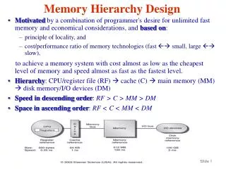
Advanced Computer Architecture Memory Hierarchy Design. Course 5MD00 Henk Corporaal November 2013 h.corporaal@tue.nl. Welcome!. This lecture: Memory Hierarchy Design Hierarchy Recap of Caching (App B) Many Cache and Memory Hierarchy Optimizations VM: virtual memory support

andie
Download Presentation

Advanced Computer Architecture Memory Hierarchy Design

An Image/Link below is provided (as is) to download presentation Download Policy: Content on the Website is provided to you AS IS for your information and personal use and may not be sold / licensed / shared on other websites without getting consent from its author. Content is provided to you AS IS for your information and personal use only. Download presentation by click this link. While downloading, if for some reason you are not able to download a presentation, the publisher may have deleted the file from their server. During download, if you can't get a presentation, the file might be deleted by the publisher.

E N D

Presentation Transcript


  1. Advanced Computer ArchitectureMemory Hierarchy Design

    Course 5MD00 HenkCorporaal November 2013 h.corporaal@tue.nl
  2. Welcome! This lecture: Memory Hierarchy Design Hierarchy Recap of Caching (App B) Many Cache and Memory Hierarchy Optimizations VM: virtual memory support AMR Cortex-A8 and Intel Core i7 examples Material: Book of Hennessy & Patterson appendix B + chapter 2: 2.1-2.6
  3. Registers vs. Memory Arithmetic instructions operands must be registers, — only 32 registers provided (Why?) Compiler associates variables with registers Question: what to do about programs with lots of variables ? Fast (2000Mhz) Slower (500Mhz) Slowest (133Mhz) Main Memory 4 Gigabyte CPU Cache Memory 1MB register file 32x4 = 128 byte registerfile
  4. Memory Hierarchy
  5. Why does a small cache still work? LOCALITY Temporal: you are likely accessing the same address soon again Spatial: you are likely accessing another address close to the current one in the near future
  6. Memory Performance Gap
  7. Memory Hierarchy Design Memory hierarchy design becomes more crucial with recent multi-core processors: Aggregate peak bandwidth grows with # cores: Intel Core i7 can generate two references per core per clock Four cores and 3.2 GHz clock 25.6 billion 64-bit data references/second + 12.8 billion 128-bit instruction references = 409.6 GB/s! DRAM bandwidth is only 6% of this (25 GB/s) Requires: Multi-port, pipelined caches Two levels of cache per core Shared third-level cache on chip
  8. Memory Hierarchy Basics Note that speculative and multithreaded processors may execute other instructions during a miss Reduces performance impact of misses
  9. Cache operation Cache / Higher level Memory / Lower level block / line tags data
  10. Direct Mapped Cache Mapping: address is modulo the number of blocks in the cache
  11. Review: Four Questions for Memory Hierarchy Designers Q1: Where can a block be placed in the upper level? (Block placement) Fully Associative, Set Associative, Direct Mapped Q2: How is a block found if it is in the upper level? (Block identification) Tag/Block Q3: Which block should be replaced on a miss? (Block replacement) Random, FIFO, LRU Q4: What happens on a write? (Write strategy) Write Back or Write Through (with Write Buffer)
  12. Direct Mapped Cache Address (bit positions) 3 1 3 0 1 3 1 2 1 1 2 1 0 Q:What kind of locality are we taking advantage of? B y t e o f f s e t 1 0 2 0 H i t D a t a T a g I n d e x I n d e x V a l i d T a g D a t a 0 1 2 1 0 2 1 1 0 2 2 1 0 2 3 2 0 3 2
  13. Direct Mapped Cache Taking advantage of spatial locality: Address (bit positions)
  14. Cache Basics cache_size = Nsets x Assoc x Block_size block_address = Byte_address DIV Block_size in bytes index = Block_address MOD Nsets Because the block size and the number of sets are (usually) powers of two, DIV and MOD can be performed efficiently block address block offset tag index 31 … … 2 1 0
  15. 6 basic cache optimizations(App. B.3) Reduces miss rate Larger block size Bigger cache Associative cache (higher associativity) reduces conflict rate Reduce miss penalty Multi-level caches Give priority to read misses over write misses Reduce hit time Avoid address translation during indexing of the cache
  16. Improving Cache Performance T = Ninstr * CPI * Tcycle CPI (with cache) = CPI_base + CPI_cachepenalty CPI_cachepenalty = ............................................. Reduce the miss penalty Reduce the miss rate Reduce the time to hit in the cache
  17. 1. Increase Block Size
  18. 2. Larger Caches Increase capacity of cache Disadvantages : longer hit time (may determine processor cycle time!!) higher cost access requires more energy
  19. 3. Use / Increase Associativity Direct mapped caches have lots of conflict misses Example suppose a Cache with 128 entries, 4 words/entry Size is 128 x 16 = 2k Bytes Many addresses map to the same entry, e.g. Byte addresses 0-15, 2k - 2k+15, 4k - 4k+15, etc. all map to entry 0 What if program accesses repeatedly (in a loop) following 3 addresses: (0, 2k+4, and 4k+12)  they will all miss, although only 3 words of the cache are really used !!
  20. Way 3 Set 1 A 4-Way Set-Associative Cache 4-ways: Set contains 4 blocks Fully associative cache contains 1 set, containing all blocks
  21. Example 1: cache calculations Assume Cache of 4K blocks 4 word block size 32 bit address Direct mapped (associativity=1) : 16 bytes per block = 2^4 32 bit address : 32-4=28 bits for index and tag #sets=#blocks/ associativity : log2 of 4K=12 : 12 for index Total number of tag bits : (28-12)*4K=64 Kbits 2-way associative #sets=#blocks/associativity : 2K sets 1 bit less for indexing, 1 bit more for tag Tag bits : (28-11) * 2 * 2K=68 Kbits 4-way associative #sets=#blocks/associativity : 1K sets 1 bit less for indexing, 1 bit more for tag Tag bits : (28-10) * 4 * 1K=72 Kbits
  22. Example 2: cache mapping 3 caches consisting of 4 one-word blocks: Cache 1 : fully associative Cache 2 : two-way set associative Cache 3 : direct mapped Suppose followingsequence of block addresses: 0, 8, 0, 6, 8
  23. Example 2: Direct Mapped Coloured = new entry = miss
  24. Example 2: 2-way Set Associative: 2 sets (so all in set/location 0) LEAST RECENTLY USED BLOCK
  25. Example 2: Fully associative (4 way assoc., 1 set)
  26. Classifying Misses: the 3 Cs The 3 Cs: Compulsory—First access to a block is always a miss. Also called cold start misses misses in infinite cache Capacity—Misses resulting from the finite capacity of the cache misses in fully associative cache with optimal replacement strategy Conflict—Misses occurring because several blocks map to the same set. Also called collision misses remaining misses
  27. 3 Cs: Compulsory, Capacity, Conflict In all cases, assume total cache size not changed What happens if we: 1) Change Block Size: Which of 3Cs is obviously affected? compulsory 2) Change Cache Size: Which of 3Cs is obviously affected? capacity misses 3) Introduce higher associativity : Which of 3Cs is obviously affected? conflict misses
  28. 3Cs Absolute Miss Rate (SPEC92) Conflict Miss rate per type
  29. 3Cs Relative Miss Rate Conflict Miss rate per type
  30. Improving Cache Performance Reduce the miss penalty Reduce the miss rate / number of misses Reduce the time to hit in the cache
  31. 4. Second Level Cache (L2) Most CPUs have an L1 cache small enough to match the cycle time (reduce the time to hit the cache) have an L2 cache large enough and with sufficient associativity to capture most memory accesses (reduce miss rate) L2 Equations, Average Memory Access Time (AMAT): AMAT = Hit TimeL1 + Miss RateL1 x Miss PenaltyL1 Miss PenaltyL1 = Hit TimeL2 + Miss RateL2 x Miss PenaltyL2 AMAT = Hit TimeL1 +Miss RateL1x (Hit TimeL2 +Miss RateL2x MissPenaltyL2) Definitions: Local miss rate— misses in this cache divided by the total number of memory accessesto this cache (Miss rateL2) Global miss rate—misses in this cache divided by the total number of memory accesses generated by the CPU(Miss RateL1 x Miss RateL2)
  32. 4. Second Level Cache (L2) Suppose processor with base CPI of 1.0 Clock rate of 500 Mhz Main memory access time : 200 ns Miss rate per instruction primary cache : 5% What improvement with second cache having 20ns access time, reducing miss rate to memory to 2% ? Miss penalty : 200 ns/ 2ns per cycle=100 clock cycles Effective CPI=base CPI+ memory stall per instruction = ? 1 level cache : total CPI=1+5%*100=6 2 level cache : a miss in first level cache is satisfied by second cache or memory Access second level cache : 20 ns / 2ns per cycle=10 clock cycles If miss in second cache, then access memory : in 2% of the cases Total CPI=1+primary stalls per instruction +secondary stalls per instruction Total CPI=1+5%*10+2%*100=3.5 Machine with L2 cache : 6/3.5=1.7 times faster
  33. 4. Second Level Cache Global cache miss is similar to single cache miss rate of second level cache provided L2 cache is much bigger than L1. Local cache rate is NOT good measure of secondary caches as it is function of L1 cache. Global cache miss rate should be used.
  34. 4. Second Level Cache
  35. 5. Read Priority over Write on Miss Write-through with write buffers can cause RAW data hazards: SW 512(R0),R3 ; Mem[512] = R3 LW R1,1024(R0) ; R1 = Mem[1024] LW R2,512(R0) ; R2 = Mem[512] Problem: if write buffer used, final LW may read wrong value from memory !! Solution 1 : Simply wait for write buffer to empty increases read miss penalty (old MIPS 1000 by 50% ) Solution 2 : Check write buffer contents before read: if no conflicts, let read continue Map to same cache block
  36. 5. Read Priority over Write on Miss What about write-back? Dirty bit: whenever a write is cached, this bit is set (made a 1) to tell the cache controller "when you decide to re-use this cache line for a different address, you need to write the current contents back to memory” What if read-miss: Normal: Write dirty block to memory, then do the read Instead:Copy dirty block to a write buffer, then do the read, then the write Fewer CPU stalls since restarts as soon as read done
  37. 6. No address translation during cache access
  38. 11 Advanced Cache Optimizations (2.2) Reducing hit time Small and simple caches Way prediction Trace caches Increasing cache bandwidth Pipelined caches Multibanked caches Nonblocking caches Reducing Miss Penalty Critical word first Merging write buffers Reducing Miss Rate Compiler optimizations Reducing miss penalty or miss rate via parallelism Hardware prefetching Compiler prefetching
  39. 1. Small and simple first level caches Critical timing path: addressing tag memory, then comparing tags, then selecting correct set Direct-mapped caches can overlap tag compare and transmission of data Lower associativity reduces power because fewer cache lines are accessed, and less complex mux to select the right way
  40. Way 3 Set 2 Recap: 4-Way Set-Associative Cache
  41. L1 Size and Associativity Access time vs. size and associativity
  42. L1 Size and Associativity Energy per read vs. size and associativity
  43. Hit Time Miss Penalty Way-Miss Hit Time 2. Fast Hit via Way Prediction Make set-associative caches faster Keep extra bits in cache to predict the “way,” or block within the set, of next cache access. Multiplexor is set early to select desired block, only 1 tag comparison performed Miss  first check other blocks for matches in next clock cycle Accuracy  85% Saves also energy Drawback: CPU pipeline is hard if hit takes 1 or 2 cycles
  44. Way Predicting Instruction Cache (Alpha 21264-like) Jump target 0x4 Jump control Add PC addr inst Primary Instruction Cache way Sequential Way Branch Target Way
  45. BR BR BR 3. Fast (Inst. Cache) Hit via Trace Cache Key Idea: Pack multiple non-contiguous basic blocks into one contiguous trace cache line instruction trace: BR BR BR trace cache line: Single fetch brings in multiple basic blocks Trace cache indexed by start address and next n branch predictions
  46. 3. Fast Hit times via Trace Cache Trace cache in Pentium 4 and its successors Dynamic instr. traces cached (in level 1 cache) Cache the micro-ops vs. x86 instructions Decode/translate from x86 to micro-ops on trace cache miss + better utilize long blocks (don’t exit in middle of block, don’t enter at label in middle of block) - complicated address mapping since addresses no longer aligned to power-of-2 multiples of word size - instructions may appear multiple times in multiple dynamic traces due to different branch outcomes
  47. 4. Pipelining Cache Pipeline cache access to improve bandwidth Examples: Pentium: 1 cycle Pentium Pro – Pentium III: 2 cycles Pentium 4 – Core i7: 4 cycles Increases branch mis-prediction penalty Makes it easier to increase associativity
  48. 5. Multi-banked Caches Organize cache as independent banks to support simultaneous access ARM Cortex-A8 supports 1-4 banks for L2 Intel i7 supports 4 banks for L1 and 8 banks for L2 Interleave banks according to block address
  49. 5. Multi-banked caches Banking works best when accesses naturally spread themselves across banks  mapping of addresses to banks affects behavior of memory system Simple mapping that works well is “sequential interleaving” Spread block addresses sequentially across banks E.g., with 4 banks, Bank 0 has all blocks with address%4 = 0; Bank 1 has all blocks whose address%4 = 1; …
  50. 6. Nonblocking Caches Allow hits before previous misses complete “Hit under miss” “Hit under multiple miss” L2 must support this In general, processors can hide L1 miss penalty but not L2 miss penalty Requires OoO processor Makes cache control much more complex
  51. Non-blocking cache
  52. 7. Critical Word First, Early Restart Critical word first Request missed word from memory first Send it to the processor as soon as it arrives Early restart Request words in normal order Send missed work to the processor as soon as it arrives Effectiveness of these strategies depends on block size and likelihood of another access to the portion of the block that has not yet been fetched
  53. 8. Merging Write Buffer When storing to a block that is already pending in the write buffer, update write buffer Reduces stalls due to full write buffer Do not apply to I/O addresses No write buffering Write buffering
  54. 9. Compiler Optimizations Loop Interchange Swap nested loops to access memory in sequential order Blocking Instead of accessing entire rows or columns, subdivide matrices into blocks Requires more memory accesses but improves locality of accesses
  55. 9. Reducing Misses by Compiler Optimizations Instructions Reorder procedures in memory so as to reduce conflict misses Profiling to look at conflicts(using developed tools) Data Merging Arrays: improve spatial locality by single array of compound elements vs. 2 arrays Loop Interchange: change nesting of loops to access data in order stored in memory Loop Fusion: combine 2 independent loops that have same looping and some variables overlap Blocking: Improve temporal locality by accessing “blocks” of data repeatedly vs. going down whole columns or rows Huge miss reductions possible !!
  56. Merging Arrays int val[SIZE]; struct record{ int key[SIZE]; int val; int key; for (i=0; i<SIZE; i++){ }; key[i] = newkey; struct record records[SIZE]; val[i]++; } for (i=0; i<SIZE; i++){ records[i].key = newkey; records[i].val++; } Reduces conflicts between val & key and improves spatial locality
  57. Loop Interchange for (col=0; col<100; col++) for (row=0; row<5000; row++) X[row][col] = X[row][col+1]; for (row=0; row<5000; row++) for (col=0; col<100; col++) X[row][col] = X[row][col+1]; Sequential accesses instead of striding through memory every 100 words Improves spatial locality columns rows array X
  58. Loop Fusion for (i = 0; i < N; i++) for (j = 0; j < N; j++) a[i][j] = 1/b[i][j] * c[i][j]; for (i = 0; i < N; i++) for (j = 0; j < N; j++) d[i][j] = a[i][j] + c[i][j]; for (i = 0; i < N; i++) for (j = 0; j < N; j++){ a[i][j] = 1/b[i][j] * c[i][j]; d[i][j] = a[i][j] + c[i][j]; } Splitted loops: every access to a and c misses. Fused loops: only 1st access misses. Improvestemporal locality Reference can be directly to register
  59. Blocking (Tiling) applied to array multiplication for (i=0; i<N; i++) for (j=0; j<N; j++){ c[i][j] = 0.0; for (k=0; k<N; k++) c[i][j] += a[i][k]*b[k][j]; } c = a The twoinnerloops: Read all NxN elements of b Read all N elements of one row of a repeatedly Write all N elements of one row of c If a whole matrix does not fit in the cache many cache misses result. Idea: compute on BxBsubmatrix that fits in the cache x b
  60. Blocking Example for (ii=0; ii<N; ii+=B) for (jj=0; jj<N; jj+=B) for (i=ii; i<min(ii+B-1,N); i++) for (j=jj; j<min(jj+B-1,N); j++){ c[i][j] = 0.0; for (k=0; k<N; k++) c[i][j] += a[i][k]*b[k][j]; } B is called Blocking Factor Can reduce capacity misses from 2N3 + N2 to 2N3/B +N2 c = a x b
  61. Reducing Conflict Misses by Blocking Conflict misses in caches vs. Blocking size Lam et al [1991]: a blocking factor of 24 had a fifth the misses compared to 48, despite both fit in cache
  62. Summary of Compiler Optimizations to Reduce Cache Misses (by hand)
  63. 10. Hardware Data Prefetching Prefetch-on-miss: Prefetch block (b + 1) upon miss on b One Block Lookahead (OBL) scheme Initiate prefetch for block (b + 1) when block b is accessed Why is this different from doubling block size? Can extend to N block lookahead Stridedprefetch If observed sequence of accesses to block: b, b+N, b+2N, then prefetch b+3N etc. Example: IBM Power 5 [2003] supports eight independent streams of stridedprefetch per processor, prefetching 12 lines ahead of current access Note: instructions are usually prefetched in instr. buffer
  64. 10. Hardware Prefetching Fetch two blocks on miss (include next sequential block) Pentium 4 Pre-fetching
  65. Issues in HW Prefetching Usefulness – should produce hits if you are unlucky, the pretetched data/instr is not needed Timeliness – not too late and not too early Cache and bandwidth pollution L1 Instruction Unified L2 Cache CPU L1 Data RF Prefetched data
  66. Prefetched instruction block Req block Stream Buffer Unified L2 Cache CPU L1 Instruction Req block RF Issues in HW prefetching: stream buffer Instruction prefetch in Alpha AXP 21064 Fetch two blocks on a miss; the requested block (i) and the next consecutive block (i+1) Requested block placed in cache, and next block in instruction stream buffer If miss in cache but hit in stream buffer, move stream buffer block into cache and prefetch next block (i+2)
  67. 11. Compiler Prefetching Insert prefetch instructions before data is needed Non-faulting: prefetch doesn’t cause exceptions Register prefetch Loads data into register Cache prefetch Loads data into cache Combine with loop unrolling and software pipelining Cost of prefetching: more bandwidth (speculation) !!
  68. Memory Technology Performance metrics Latency is concern of cache Bandwidth is concern of multiprocessors and I/O Access time Time between read request and when desired word arrives Cycle time Minimum time between unrelated requests to memory DRAM used for main memory, SRAM used for cache
  69. Memory Technology SRAM Requires low power to retain bit Requires 6 transistors/bit DRAM Must be re-written after being read Must also be periodically refeshed Every ~ 8 ms Each row can be refreshed simultaneously One transistor/bit Address lines are multiplexed: Upper half of address: row access strobe (RAS) Lower half of address: column access strobe (CAS)
  70. Memory Technology Amdahl: Memory capacity should grow linearly with processor speed Unfortunately, memory capacity and speed has not kept pace with processors Some optimizations: Multiple accesses to same row Synchronous DRAM Added clock to DRAM interface Burst mode with critical word first Wider interfaces Double data rate (DDR) Multiple banks on each DRAM device
  71. SRAM vs DRAM A bit is stored as charge on the capacitor Bit cell loses charge over time (read operation and circuit leakage) Must periodically refresh Hence the name DynamicRAM Static Random Access Memory Dynamic Random Access Memory Bitlines driven by transistors - Fast (10x) 1 transistor and 1 capacitor vs. 6 transistors Large (~6-10x) Credits: J.Leverich, Stanford
  72. DRAM: Internal architecture Bit cells are arranged to form a memory array Multiple arrays are organized as different banks Typical number of banks are 4, 8 and 16 Sense amplifiers raise the voltage level on the bitlines to read the data out Bank 4 Bank 3 Bank 2 Bank 1 Address register Address MS bits Row decoder Memory Array Row Buffer Row Buffer Row Buffer Sense amplifiers (row buffer) LS bits Column decoder Data Credits: J.Leverich, Stanford
  73. Memory Optimizations
  74. Memory Optimizations
  75. Memory Optimizations DDR: DDR2 Lower power (2.5 V -> 1.8 V) Higher clock rates (266 MHz, 333 MHz, 400 MHz) DDR3 1.5 V 800 MHz DDR4 1-1.2 V 1600 MHz GDDR5 is graphics memory based on DDR3
  76. Memory Optimizations Graphics memory: Achieve 2-5 X bandwidth per DRAM vs. DDR3 Wider interfaces (32 vs. 16 bit) Higher clock rate Possible because they are attached via soldering instead of socketted DIMM modules Reducing power in SDRAMs: Lower voltage Low power mode (ignores clock, continues to refresh)
  77. Memory Power Consumption
  78. Flash Memory Type of EEPROM (Electrical Erasable Programmable Read Only Memory) Must be erased (in blocks) before being overwritten Non volatile Limited number of write cycles Cheaper than SDRAM, more expensive than disk Slower than SRAM, faster than disk
  79. Memory Dependability Memory is susceptible to cosmic rays Soft errors: dynamic errors Detected and fixed by error correcting codes (ECC) Hard errors: permanent errors Use sparse rows to replace defective rows Chipkill: a RAID-like error recovery technique
  80. Virtual Memory Protection via virtual memory Keeps processes in their own memory space Role of architecture: Provide user mode and supervisor mode Protect certain aspects of CPU state Provide mechanisms for switching between user and supervisor mode Provide mechanisms to limit memory accesses read-only pages executable pages shared pages Provide TLB to translate addresses
  81. Memory organization The operating system, together with the MMU hardware, take care of separating the programs. Each program runs in its own ‘virtual’ environment, and uses logical addressing that is (often) different the the actual physical addresses. Within the virtual world of a program, the full 4 Gigabytes address space is available. (Less under Windows) In the von Neumann architecture, we need to manage the memory space to store the following: The machine code of the program The data: Global variables and constants The stack/local variables The heap Main memory Program + Data
  82. Memory Organization: more detail The memory that is reservedby the memory manager 0xFFFFFFFF Heap Variable size If the heap and thestack collide, we’re out of memory The local variables in the routines. With each routine call, a new set of variablesif put in the stack. Free memory Stack pointer Before the first lineof the program is run,all global variables and constants are initialized. Variable size Stack Fixed size Global variables The program itself: a set of machine instructions.This is in the .exe Machine code Fixed size 0x00000000
  83. Memory management Swap file on hard disk Problem: many programs run simultaneously MMU manages the memory access. Memory Management Unit Main memory No: accessviolation 2K block 2K block No: load 2K blockfrom swap fileon disk CPU 2K block Logicaladdress Processtable Yes: VirtualMemoryManager Physical address 2K block 2K block Yes: Physical address Physical address Cache memory 2K block 2K block 2K block Each program thinksthat it owns all thememory. Checks whether therequested addressis ‘in core’
  84. Virtual Memory Main memory can act as a cache for the secondary storage (disk) physical memory virtual memory Advantages: illusion of having more physical memory program relocation protection
  85. Pages: virtual memory blocks Page faults: the data is not in memory, retrieve it from disk huge miss penalty, thus pages should be fairly large (e.g., 4KB) reducing page faults is important (LRU is worth the price) can handle the faults in software instead of hardware using write-through is too expensive so we use writeback
  86. V i r t u a l p a g e n u m b e r P a g e t a b l e P h y s i c a l m e m o r y P h y s i c a l p a g e o r d i s k a d d r e s s V a l i d 1 1 1 1 0 1 1 0 1 D i s k s t o r a g e 1 0 1 Page Tables
  87. Page Tables
  88. Size of page table Assume 40-bit virtual address; 32-bit physical 4 Kbyte pages; 4 bytes per page table entry (PTE) Solution Size = Nentries * Size-of-entry = 2 40 / 2 12 * 4 bytes = 1 Gbyte Reduce size: Dynamic allocation of page table entries Hashing: inverted page table 1 entry per physical available instead of virtual page Page the page table itself (i.e. part of it can be on disk) Use larger page size (multiple page sizes)
  89. Fast Translation Using a TLB Address translation would appear to require extra memory references One to access the PTE (page table entry) Then the actual memory access However access to page tables has good locality So use a fast cache of PTEs within the CPU Called a Translation Look-aside Buffer (TLB) Typical: 16–512 PTEs, 0.5–1 cycle for hit, 10–100 cycles for miss, 0.01%–1% miss rate Misses could be handled by hardware or software
  90. TLB Valid Tag Page address 1 Physical memory 1 Virtual page number 1 1 0 1 Physical page or disk address Valid 1 1 Disk storage 1 1 0 1 1 Page table 0 1 1 0 1 Making Address Translation Fast A cache for address translations: translation lookaside buffer (TLB)
  91. TLBs and caches V i r t u a l a d d r e s s T L B a c c e s s N o Y e s T L B m i s s T L B h i t ? e x c e p t i o n P h y s i c a l a d d r e s s N o Y e s W r i t e ? T r y t o r e a d d a t a Y e s N o f r o m c a c h e W r i t e a c c e s s b i t o n ? W r i t e p r o t e c t i o n W r i t e d a t a i n t o c a c h e , e x c e p t i o n u p d a t e t h e t a g , a n d p u t N o Y e s t h e d a t a a n d t h e a d d r e s s C a c h e m i s s s t a l l C a c h e h i t ? i n t o t h e w r i t e b u f f e r D e l i v e r d a t a t o t h e C P U
  92. Overall operation of memory hierarchy Each instruction or data access can result in three types of hits/misses: TLB, Page table, Cache Q: which combinations are possible?Check them all! (see fig 5.26)
  93. AMR Cortex-A8 data caches/TLP. Since the instruction and data hierarchies are symmetric, we show only one. The TLB (instruction or data) is fully associative with 32 entries. The L1 cache is four-way set associative with 64-byte blocks and 32 KB capacity. The L2 cache is eight-way set associative with 64-byte blocks and 1 MB capacity. This figure doesn’t show the valid bits and protection bits for the caches and TLB, nor the use of the way prediction bits that would dictate the predicted bank of the L1 cache.
  94. Intel Nehalem (i7) 13.5 x 19.6 mm Per core: 731 Mtransistors 32-KB I & 32-KB data $ 512 KB L2 2-level TLB Shared: 8 MB L3 2 128bit DDR3 channels
  95. The Intel i7 memory hierarchy The steps in both instruction and data access. We show only reads for data. Writes are similar, in that they begin with a read (since caches are write back). Misses are handled by simply placing the data in a write buffer, since the L1 cache is not write allocated.
  96. Address translation and TLBs
  97. Cache L1-L2-L3 organization
  98. Virtual Machines Supports isolation and security Sharing a computer among many unrelated users Enabled by raw speed of processors, making the overhead more acceptable Allows differentoperating systems to be presented to user programs “System Virtual Machines” SVM software is called “virtual machine monitor” or “hypervisor” Individual virtual machines run under the monitor are called “guest VMs”
  99. Impact of VMs on Virtual Memory Each guest OS maintains its own set of page tables VMM adds a level of memory between physical and virtual memory called “real memory” VMM maintains shadow page table that maps guest virtual addresses to physical addresses Requires VMM to detect guest’s changes to its own page table Occurs naturally if accessing the page table pointer is a privileged operation
More Related