Download

1 / 24
250 likes | 460 Views
Design and development of FPGA based PCI Express card. By Sunil G. Kulkarni , SO/F, Pelletron-Linac Facility, BARC-TIFR. Industry Standard Bus Throughput Comparison:. PCI transactions are packetized and then serialized GEN1 speed @ 2.5Gb/S, GEN2 speed @ 5Gb/S, GEN3 speed @ 8 Gb/S

E N D
Design and development of FPGA based PCI Express card By Sunil G. Kulkarni, SO/F, Pelletron-Linac Facility, BARC-TIFR. 21/01/2011 ASET
Industry Standard Bus Throughput Comparison: 21/01/2011 ASET
PCI transactions are packetized and then serialized • GEN1 speed @ 2.5Gb/S, GEN2 speed @ 5Gb/S, GEN3 speed @ 8 Gb/S • LVDS Signalling, point-to-point, 8B/10B encoded • Full duplex operation • Lane-wise Scalability PCI Express: Evolution of PCI 21/01/2011 ASET
High Bandwidth • Software Backward Compatibility • Layered Architecture • Next Generation I/O • I/O Simplification Advantages of PCI Express: 21/01/2011 ASET
High Bandwidth: 21/01/2011 ASET
Dedicated I/O 21/01/2011 ASET
PCI PnP Model (init, enum, config) OS Config No OS Impact PCI Software/Driver Model S/W Packet-based Protocol Transaction Data Integrity Data Link Point-to-point, serial, differential… Physical Future speeds and encoding technologies only impact physical layer Backward Compatibility 21/01/2011 ASET
PCI Express layers: 21/01/2011 ASET
Transaction layer Packet (TLP): 21/01/2011 ASET
Whether ASIC or FPGA? ASIC : Only for one and four lanes. Example: PLX 8311 (one lane bridge), NI Modules FPGA : Eight lanes support. Example : Xilinx Virtex-5 (eight lanes HARD IP) Selected Method: Xilinx Virtex-5 FPGA Implementation Options: 21/01/2011 ASET
Topology of PCIe System 21/01/2011 ASET
x8, x4, x2, or x1 lane width • RocketIO™ GTP and GTX transceivers implement a fully compliant PHY • Block RAMs used for buffering • Up to 6 x 32 bit or 3 x 64 bit base address registers (BARs) • Up to two virtual channels (VCs) Virtex-5 FPGA Integrated Endpoint Block for PCI Express Designs 21/01/2011 ASET
Endpoint Block Diagram: 21/01/2011 ASET
Clock Resources: 21/01/2011 ASET
Clock Frequency Versus Lane Width 21/01/2011 ASET
The Transmit (TX), Receive (RX), and Retry buffers are implemented with block RAM. • Transmit buffer. Buffers transmitted packets. It is divided into separate FIFOs for posted, non-posted, and completion transactions. • Receive buffer. Buffers received packets. It is divided into separate FIFOs for posted, non-posted, and completion transactions. • Retry buffer. Holds a copy of each TLP that is currently in the process of being • transmitted until the information has been received correctly Block RAM Interface 21/01/2011 ASET
This tool provides a wrapper around the integrated Endpoint block and automatically connects the block RAMs, RocketIOtransceivers, and reset and clock modules. • This is used via GUI where the user can select number of lanes, different clocks, registers and other memory devices. LogiCORE™ Endpoint Block Plus Wrapper 21/01/2011 ASET
Snapshots: 21/01/2011 ASET
Snapshots cont.. 21/01/2011 ASET
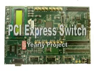
PCI Express Interface Card: 21/01/2011 ASET
PCB has 16 layers with alternate GROUND layers to avoid signal integrity issues. • All high speed tracks (PCI Express differential signals as well as differential clock signals) are simulated for impedance calculations (100 ohms) . • Differential pair lengths are matched within +-5 mils. • Board design is carried out using cadence tools and board simulations using Hyper lynx from mentor graphics. PCB Design: 21/01/2011 ASET
Higher pin counts of FPGA means higher number of PCB layers and hence higher fabrication costs. • FPGA with built-in PCI Express blocks are costly. • PCB design becomes complex and board simulations are required. • Due to above constraints , a thorough cost versus functionality audit is needed. Major Design issues: 21/01/2011 ASET
To design data acquisition system with addition of high speed ADCs/DACs on-board. • To design PXI Express based modular instruments or data acquisition modules. • To develop high speed peer-to-peer data transfer links via Fiber-optic cables. • To process or display video applications where bandwidth requirement is very high. • To design multiple FPGA board for DSP operations and transferring data to PC. Applications: 21/01/2011 ASET
ShriJaydeep Gore. • Shri P. V. Bhagwat. • Shri V. V. Tambwekar. • Dr. R. K. Shyamasundar. Acknowledgements: 21/01/2011 ASET