Download
1 / 21
230 likes | 460 Views
製作具次波長結構之大面積抗反射光學元件. Fabrication of large area sub-wavelength structures for anti-reflection optical film. Reporter ﹕Wen-Yu Lee Advisor : Cheng- Hsin Chuang Department of Mechanical Engineering, Southern Taiwan University of Science and Technology, Tainan, Taiwan Date: 2013/03/05.

E N D
製作具次波長結構之大面積抗反射光學元件 Fabrication of large area sub-wavelength structures for anti-reflection optical film Reporter ﹕Wen-Yu Lee Advisor :Cheng-Hsin Chuang Department of Mechanical Engineering, Southern Taiwan University of Science and Technology, Tainan, Taiwan Date: 2013/03/05
Outline Introduction Experimental setup and results Anti-reflection film measurement Conclusions & Future works • Motivation • Types of Anti-reflection film • Porous Anodic Alumina Oxide (AAO) Template • Nano imprinting process • The transmittance and reflectance measurement results • Comparing the results of different experiment parameters
Outline Introduction Experimental setup and results Anti-reflection film measurement Conclusions & Future works • Motivation • Types of Anti-reflection film • Porous Anodic Alumina Oxide (AAO) Template • Nano imprinting process • The transmittance and reflectance measurement results • Comparing the results of different experiment parameters
Motivation • Disadvantages of light reflection Decreased conversion efficiency Low transmittance Low contrast Reflection 10% Air n=1 Air n=1 n=1.1~1.4 n=1.5 n=1.5 Low contrast
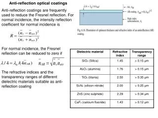
Types of Anti-reflection film • Antireflective coating technology – Multilayer coating • Antireflective structure – Sub-wavelength structure (SWSs) Protective film Antireflection layer Substrate with hard coating Adhesive layer Separator The refractive index of multilayer (Ladder) High-cost facilities
Types of Anti-reflection film • Antireflective structure - Sub-wavelength structure (SWSs) • Moth eye structures • How to achieve broadband and omnidirectionalantireflection with low cost process? The reflective index of cylindrical SWSs The reflective index of cone-shape SWSs • Sub-wavelength Structures(SWSs) • The best optical characteristic • Imprinting process • Low-cost Multilayer coating Information source : FINETECH JAPAN 2011 The lowest reflection and broadband
Types of Sub-wavelength structures (SWSs) • Colloidal lithography • Electron beam lithography • Nano imprinting technique Electron beam lithography RIE BOE etching Etching • Advantages • Low-cost nano-scale mold • Simple process • The best optical characteristic • Large area • Interference lithography KOH etching Langmuir, 2009, 25 (13), pp 7375–7382 Solar Energy Materials & Solar Cells 94 (2010) 629–633 • Disadvantages • Complex • High-end facilities • Costly • Small size Optics Communications 282 (2009) 434–438
Outline Introduction Experimental setup and results Anti-reflection film measurement Conclusions & Future works • Motivation • Types of Anti-reflection film • Porous Anodic Alumina Oxide (AAO) Template • Nano imprinting process • The transmittance and reflectance measurement results • Comparing the results of different experiment parameters
Experimental – Fabrication of AAO template • Procedures • Process condition • Constant voltage of 80V • Oxalic acid solution (0.3M) • Temperature at 4℃ Anodizing + etchig = 1 time (2nd cycle) Anodizing + etchig = 1 time (1st cycle) Acid cleaning pure Al foil Removed anodic oxide layer by acid • Phosphoric acid solution (5wt%) • Temperature at 32℃ 2ndanodization process 1stanodization process Oxalic acid solution Pure aluminum Phosphoric acid etching Schematic of the cross section Oxalic acid solution Platinum(Pt) Platinum(Pt)
Experimental result – Different 2ndanodization time • Top view High purity aluminum foil 30sec 45sec 60sec • Cross section view Aspect ratio 1:1 Aspect ratio 1:1.5 Aspect ratio 1:2 30sec 45sec 60sec
Experimental result – Different 2ndanodization time • Top view Sputtering aluminum membrane with temper, widening time 10 min 30sec 45sec • Cross section view Aspect ratio 1:1.2 Aspect ratio 1:2.5 30sec 45sec
Experimental result – Different Pore widening time • Top view Sputtering aluminum membrane with temper, widening time 10 min 10min 15min • Cross section view Aspect ratio 1:2.5 Aspect ratio 1:1.5 10min 15min
Experimental result – Compare the results of temper • Tempering status • Tempering champer 400 Rapid cooling • SEM images of AAO template Anodizing time 45sec , widening time 15 min Without temper With temper 5 ̊C / min 400̊C, 4hr
Experimental process – Nano imprinting process • AAO template with cone structure AAO template AAO template Roller UV light PET substrate UV curable Anti-reflection Film Nano imprinting Process Sub-wavelength structures PET substrate Anti-reflection Film Schematic of nanoimprinting process by using UV exposure technique.
0.5 Experimental result – Nano imprinting process by using AAO template • AAO template • SWSs Aluminum substrate Aspect ratio 1:1 Aspect ratio 1:1 Aspect ratio 1:1 Sputtering Al membrane Sputtering Al membrane (without temper) Sputtering Al membrane Aspect ratio 1:1.5 Sputtering Al membrane Aspect ratio 1:2 45sec, 10min 30sec, 10min 45sec, 15min 45sec, 15min
Outline Introduction Experimental setup and results Anti-reflection film measurement Conclusions & Future works • Motivation • Types of Anti-reflection film • Porous Anodic Alumina Oxide (AAO) Template • Nano imprinting process • The transmittance and reflectance measurement results • Comparing the results of different experiment parameters
Optical measurements results – Transmittance (%) • Transmittance and of the glass plate with/without SWSs 95.1% 94.2% Aspect ratio increased 92.9% 91.8% 89.7%
Optical measurements results – Reflectance (%) • Reflectance and of the glass plate with/without the SWSs Incident light angles 5 ̊ 15 ̊ 30 ̊ 45 ̊ 60 ̊ 0.64% Aspect ratio increased Reflectance (%) 0.26% 0.16% 1% 0.14% Wavelength (nm)
Outline Introduction Experimental setup and results Anti-reflection film measurement Conclusions & Future works • Motivation • Types of Anti-reflection film • Porous Anodic Alumina Oxide (AAO) Template • Nano imprinting process • The transmittance and reflectance measurement results • Comparing the results of different experiment parameters
Conclusions • This study successfully fabricated the large area AAO template by using homemade Circulate-coolded etching system. • In the fabrication of large area cone-shape AAO template,we could control the different depth characteristics of anodic alumina by phosphoric acid etching process and anodization parameters. • We have successfully produced sub-wavelength structures(SWSs)on glass plant by using hot embossing with AAO template • In the optical measurement results, the average transmittance of glass plate with SWSs was 96.5% and the reflection was reduced from 5.71% to 0.2%. • Due to the contact angle of high-aspect-ratio SWSs film exceeded110°, the surface energy is much lower than bare glass whose contact angle is 25°. Consequently, a SWSs film could possess the self-cleaningeffect.