Download
1 / 26
260 likes | 358 Views
SPECIFICATION FOR APPROVAL. Contents. RECORD OF REVISIONS. POWER (V cc ,GND). SOURCE DRIVE CIRCUIT. POWER SUPPLY. D1. D2. D2399. D2400. LDO (3.3V). G1. CN1. G2. GATE DRIVE CIRCUIT. TFT-LCD (800 X RGB X 480). DISPLAY DATA & TIMING SIGNAL (3.3V Level).

E N D
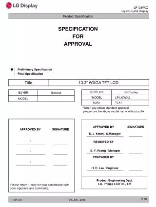
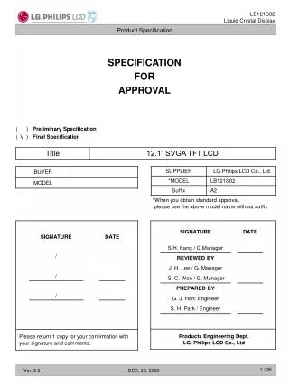
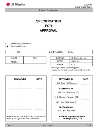
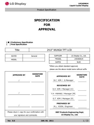
SPECIFICATION FOR APPROVAL
POWER (Vcc,GND) SOURCE DRIVE CIRCUIT POWER SUPPLY D1 D2 D2399 D2400 LDO (3.3V) G1 CN1 G2 GATE DRIVE CIRCUIT TFT-LCD (800 X RGB X 480) DISPLAY DATA & TIMING SIGNAL (3.3V Level) TIMING CONTROLLER G479 G480 INPUT CONNECTOR VBL LAMP CN2 GND 1. Summary This module utilizes amorphous silicon thin film transistors and a 16:9 aspect ratio. A 8.0” active matrix liquid crystal display allows full color to be displayed. The applications are Portable DVD, Amusement and others AV system. 2. Features • Utilizes a panel with a 16:9 aspect ratio, which makes the module suitable for use in wide-screen • systems. • The 8.0” screen produces a high resolution image that is composed of 384,000 pixel elements in a stripe • arrangement. • Wide viewing angle technology is employed. • [The most suitable viewing direction is in the 6 o’clock direction.] • By adopting an active matrix drive, a picture with high contrast is realized. • A thin, light and compact module is accomplished through the use of COG mounting technology. • By adopting a high aperture panel, high transmittance color filter and high transmission polarizing plates, • transmittance ratio is realized. • Gray scale or the brightness of the sub-pixel color is determined with a 6-bit gray scale signal. • DE(Data enable) only mode. (60Hz)
3. General Specification 4. Absolute Maximum Ratings The following are maximum values which, if exceeded, may cause faulty operation or damage to the unit. Table 1. ABSOLUTE MAXIMUM RATINGS [Note 4-1] This rating applies to all parts of the module and should not be exceeded. [Note 4-2] Maximum wet-bulb temperature is 60℃. Condensation of dew must be avoided as electrical current leaks will occur, causing a degradation of performance specifications. [Note 4-3] The operating temperature only guarantees operation of the circuit and doesn’t guarantee all the contents of Electro-optical specification.
5. Electrical Specifications 5-1. Electrical Characteristics The LB080WV3-B1 requires two power inputs. One is employed to power the LCD electronics and to drive the TFT array and liquid crystal. The second input which powers the CCFL, is typically generated by an inverter. The inverter is an external unit to the LCD. Table 2. ELECTRICAL CHARACTERISTICS Note) The design of the inverter must have specifications for the lamp in LCD Assembly. The performance of the Lamp in LCM, for example life time or brightness, is extremely influenced by the characteristics of the DC-AC inverter. So all the parameters of an inverter should be carefully designed so as not to produce too much leakage current from high-voltage output of the inverter. When you design or order the inverter, please make sure unwanted lighting caused by the mismatch of the lamp and the inverter(no lighting, flicker, etc) never occurs. When you confirm it, the LCD Assembly should be operated in the same condition as installed in your instrument. * 1. VCC=5.0V, 25C, fV (frame frequency) = 60Hz condition, whereas mosaic pattern(Typ),full black pattern(Max) is displayed. [LDO output voltage(3.3V) is applied.] * 2. This frequency range means the range to keep within ±10% change of electrical and optical characteristics. * 3. This frequency range means not affecting to lamp life and reliability characteristics. (The lamp frequency should be selected as different as possible from display horizontal synchronous signal (Including harmonic frequency of this scanning frequency) to avoid “Beat” interference which may be observed on the screen as horizontal stripes like moving wave.
I p I -p . This phenomenon is caused by interference between lamp (CCFL) lighting frequency and LCD horizontal synchronous signal.) * 4. The “MAX” of “Kick-Off Voltage” means the minimum voltage for inverter to turn on the CCFL normally in the LCD module. However this isn’t the values that we can assure stability of starting lamp on condition that the module is installed in your set. It should be careful that “Kick-Off Voltage” is changed by an increase of stray capacitance in your set, inverter method, value of ballast capacitor in your inverter and so on. Especially, the value of “Kick-Off Voltage” is higher in low temperature condition than in normal temperature condition, because impedance of CCFL is increased. The voltage above VS should be applied to the lamps for more than 1 second for start-up. Otherwise, the lamps may not be turned on. The used lamp current is the lamp typical current. * 5. The time needed to achieve not less than 95%brightness of the center part of lamp. The brightness of the lamp after being lighted for 5 minutes is defined as 100%. * 6. “Life time” is defined as the time that the lamp brightness decreases to 50% from original brightness at IBL=TYP; continuous lighting, Ta=25℃. . Requirements for a system inverter design, which is intended to have a better display performance, a better power efficiency and a more reliable lamp, are as follows. It shall help increase the lamp lifetime and reduce leakage current. Inverter should be designed to be subject to the conditions below A. The asymmetry rate of the inverter waveform should be less than 10%. B. The distortion rate of the waveform should be within 2 10%. * Inverter output waveform had better be more similar to ideal sine wave. C. There should not be any spikes in the waveform. D. Lamp current should not exceed the “MAX” value under the “Operating Temperature” (it is prohibited to exceed the “MAX.” value even if it is operated in the guaranteed temperature). When lamp current exceed the maximum value for a long time, it may cause a smoking and Ignition. Therefore, it is recommended that the inverter have the current limited circuit that is used as a protection circuit and/or the lamp current-controlled inverter. • * Asymmetry rate: • ( I p – I –p |) / Irms * 100% • Distortion rate: • I p (or I –p) / Irms Do not attaches a conducting tape to lamp connecting wire. If the lamp wire attach to a conducting tape, TFT-LCD Module has a low luminance and the inverter has abnormal action. Because leakage current is occurred between lamp wire and conducting tape. 5-2. Interface Connections This LCD employs Two interface connections, a 40 pin connector is used for the module electronics interface and the other connectors is used for the integral backlight system. The electronics interface connector is a model FH12K-40S-0.5SH manufactured by HIROSE.
Pin Symbol Description Notes 1 2 3 4 5 6 7 8 9 10 11 12 13 14 15 16 17 18 19 20 21 22 23 24 25 26 27 28 29 30 31 32 33 34 35 36 37 38 39 40 VSS VSS B5 B4 B3 VSS B2 B1 B0 VSS G5 G4 G3 VSS G2 G1 G0 VSS R5 R4 R3 VSS R2 R1 R0 VSS DE VSS L_R U_D VSS DCLK RBF VSS VCC VCC VCC VCC VSS VSS Connect to VSS, see Note 1 Connect to VSS, see Note 1 Blue data most significant bit(MSB) Connect to VSS, see Note 1 Blue data least significant bit(LSB) Connect to VSS, see Note 1 Green data most significant bit(MSB) Connect to VSS, see Note 1 Green data least significant bit(LSB) Connect to VSS, see Note 1 Red data most significant bit(MSB) Connect to VSS, see Note 1 Red data least significant bit(LSB) Connect to VSS, see Note 1 Data Enable Timing Signal Connect to VSS, see Note 1 Connect to VSS, see Note 1 Connect to VSS, see Note 1 +5.0Vdc power supply input, see Note 2 +5.0Vdc power supply input, see Note 2+5.0Vdc power supply input, see Note 2 +5.0Vdc power supply input, see Note 2 Connect to VSS, see Note 1 Connect to VSS, see Note 1 Table 3. MODULE CONNECTOR PIN CONFIGURATION (CN1) Ground Ground Blue data Blue data Blue data Ground Blue data Blue data Blue data Ground Green data Green data Green data Ground Green data Green data Green data Ground Red data Red data Red data Ground Red data Red data Red data Ground Data Enable Ground Left/Right Scanning Change Up/Down Scanning Change Ground Data Clock No Connection Ground Power input Power input Power input Power input Ground Ground Note : 1. All VSS(Ground) pins should be connected together and the LCD’s metal frame. 2. All VCC(Power input) pins should be connected together.
Table 4. BACKLIGHT CONNECTOR PIN CONFIGURATION The backlight interface connector is a model BHSR-02VS-1 manufactured by JST or a compatible model manufactured by AMP. The matching connector part number is SM02B-BHSS-1-TB manufactured by JST or equivalent. 1. The wire color of high voltage side is pink. 2. The wire color of low voltage side is white. Connect the low voltage side of the DC/AC inverter used to drive the fluorescent tube to GND of the inverter circuit.
5-3. Signal Timing Specifications Table 5. TIMING TABLE
tHr,tVr tIr,tDr tHf,tVf tIf,tDf 0.7Vdd 3.3V(Vdd) 0.3Vdd DCLK, Hsync, Vsync, DE, DATA tWCH tWCL tfCLK trCLK tCLK 0.5Vdd DCLK tHD tSD tCLKL DATA Invalid Data Invalid Data tSI tHI DE DCLK tHH tSH Hsync tHV tSV Vsync tHP tWH Hsync tHBP tHFP tHDP DE tVP tWV Vsync tVBP tVDP tVFP DE 5-4. Signal Timing Waveforms [Vdd = 3.3V]
5-5. Color Input Data Reference The brightness of each primary color (red,green and blue) is based on the 6-bit gray scale data input for the color ; the higher the binary input, the brighter the color. The table below provides a reference for color versus data input. Table 6. COLOR DATA REFERENCE
Power supply for LCD ( VCC) Interface Signal (Tx) Power for Lamp 5-6. Power Sequence Table 7. POWER SEQUENCE TABLE Note) 1. Please avoid floating state of interface signal at invalid period. 2. When the interface signal is invalid, be sure to pull down the power supply for LCD VCC to 0V. 3. Lamp power must be turn on after power supply for LCD and interface signal are valid.
6. Optical Specification Optical characteristics are determined after the unit has been ‘ON’ and stable for approximately 30 minutes in a dark environment at 25C. The values specified are at an approximate distance 50cm from the LCD surface at a viewing angle of and equal to 0. FIG. 1 presents additional information concerning the measurement equipment and method. FIG. 1 Optical Characteristic Measurement Equipment and Method LCD Module Pritchard 880 or equivalent Optical Stage(x,y) 50cm Table 8. OPTICAL CHARACTERISTICS Ta=25C, VCC=5.0V, fV=60Hz, Dclk= 32MHz, IL=6.0mA
Note) 1. Contrast Ratio(CR) is defined mathematically as Surface Luminance with all white pixels Contrast Ratio = Surface Luminance with all black pixels 2. Surface luminance is the center point across the LCD surface 50cm from the surface with all pixels displaying white. For more information see FIG 1. 3. The variation in surface luminance , The Panel total variation ( WHITE) is determined by measuring LN at each test position 1 through 5, and then dividing the maximum LN of 5 points luminance by minimum LN of 5 points luminance. For more information see FIG 2. WHITE = Maximum(L1,L2, … L5) / Minimum(L1,L2, … L5) 4. Response time is the time required for the display to transition from white to black (rise time, TrR) and from black to white(Decay Time, TrD). For additional information see FIG 3. 5. Viewing angle is the angle at which the contrast ratio is greater than 10. The angles are determined for the horizontal or x axis and the vertical or y axis with respect to the z axis which is normal to the LCD surface. For more information see FIG 4.
H H/2 H/4 V/4 V/2 V Center Point H,V : ACTIVE AREA L4 L2 L3 L5 L1 Tr Tr D R % 100 90 Optical Response 10 0 white white black FIG. 2 Luminance <measuring point for surface luminance & measuring point for luminance variation> FIG. 3 Response Time The response time is defined as the following figure and shall be measured by switching the input signal for “black” and “white”.
FIG. 4 Viewing angle <Dimension of viewing angle range> [FPC Side]
7. Mechanical Characteristics The contents provide general mechanical characteristics for the model LB080WV3-B1. In addition the figures in the next page are detailed mechanical drawing of the LCD.
<FRONT VIEW> Note) Unit:[mm], General tolerance: 0.5mm
<REAR VIEW> Note) Unit:[mm], General tolerance: 0.5mm
8. Reliability Note) 1. Ta= Ambient Temperature. 2. In the normal condition after test, there shall be no display NG issue occurred. All the cosmetic specification is judged before the reliability stress.
9. International Standards 9-1. Safety a) UL 60950, Third Edition, Underwriters Laboratories, Inc., Dated Dec. 11, 2000. Standard for Safety of Information Technology Equipment, Including Electrical Business Equipment. b) CAN/CSA C22.2, No. 60950, Third Edition, Canadian Standards Association, Dec. 1, 2000. Standard for Safety of Information Technology Equipment, Including Electrical Business Equipment. c) EN 60950 : 2000, Third Edition IEC 60950 : 1999, Third Edition European Committee for Electrotechnical Standardization(CENELEC) EUROPEAN STANDARD for Safety of Information Technology Equipment Including Electrical Business Equipment. 9-2. EMC a) ANSI C63.4 “Methods of Measurement of Radio-Noise Emissions from Low-Voltage Electrical and Electrical Equipment in the Range of 9kHZ to 40GHz. “American National Standards Institute(ANSI), 1992 b) C.I.S.P.R “Limits and Methods of Measurement of Radio Interface Characteristics of Information Technology Equipment.“ International Special Committee on Radio Interference. c) EN 55022 “Limits and Methods of Measurement of Radio Interface Characteristics of Information Technology Equipment.“ European Committee for Electrotechnical Standardization.(CENELEC), 1998 ( Including A1: 2000 )
A B C D E F G H I J K L M Month Jan Feb Mar Apr May Jun Jul Aug Sep Oct Nov Dec Mark 1 2 3 4 5 6 7 8 9 A B C Year 1 ~ 99999 100000 ~ Year 97 98 99 2000 2001 2002 2003 2004 2005 2006 2007 Mark 00001 ~ 99999 A0001 ~ A9999, ..... , Z9999 Mark 7 8 9 0 1 2 3 4 5 6 7 10. Packing 10-1. Designation of Lot Mark a) Lot Mark A,B,C : SIZE(INCH) D : YEAR E : MONTH F : PANEL CODE G : FACTORY CODE H : ASSEMBLY CODE I,J,K,L,M : SERIAL NO. Note 1. YEAR 2. MONTH 3. PANEL CODE 4. FACTORY CODE 5. SERIAL NO. b) Location of Lot Mark Serial NO. is printed on the label. The label is attached to the backside of the LCD module. This is subject to change without prior notice. 10-2. Packing Form a) Package quantity in one box : 28 pcs b) Box Size : 333 x 282 x 280 (mm)
11. PRECAUTIONS Please pay attention to the following when you use this TFT LCD module. 11-1. MOUNTING PRECAUTIONS (1) You must mount a module using holes arranged in four corners or four sides. (2) You should consider the mounting structure so that uneven force(ex. Twisted stress) is not applied to the module. And the case on which a module is mounted should have sufficient strength so that external force is not transmitted directly to the module. (3) Please attach a transparent protective plate to the surface in order to protect the polarizer. Transparent protective plate should have sufficient strength in order to the resist external force. (4) You should adopt radiation structure to satisfy the temperature specification. (5) Acetic acid type and chlorine type materials for the cover case are not desirable because the former generates corrosive gas of attacking the polarizer at high temperature and the latter causes circuit break by electro-chemical reaction. (6) Do not touch, push or rub the exposed polarizers with glass, tweezers or anything harder than HB pencil lead. And please do not rub with dust clothes with chemical treatment. Do not touch the surface of polarizer for bare hand or greasy cloth.(Some cosmetics deteriorate the polarizer.) (7) When the surface becomes dusty, please wipe gently with absorbent cotton or other soft materials like chamois soaks with petroleum benzine. Normal-hexane is recommended for cleaning the adhesives used to attach front / rear polarizers. Do not use acetone, toluene and alcohol because they cause chemical damage to the polarizer. (8) Wipe off saliva or water drops as soon as possible. Their long time contact with polarizer causes deformations and color fading. (9) Do not open the case because inside circuits do not have sufficient strength. (10) The metal case of a module should be contacted to electrical ground of your system. 11-2. OPERATING PRECAUTIONS (1) The spike noise causes the mis-operation of circuits. It should be lower than following voltage : V=±200mV(Over and under shoot voltage) (2) Response time depends on the temperature.(In lower temperature, it becomes longer.) (3) Brightness depends on the temperature. (In lower temperature, it becomes lower.) And in lower temperature, response time(required time that brightness is stable after turned on) becomes longer. (4) Be careful for condensation at sudden temperature change. Condensation makes damage to polarizer or electrical contacted parts. And after fading condensation, smear or spot will occur. (5) When fixed patterns are displayed for a long time, remnant image is likely to occur. (6) Module has high frequency circuits. Sufficient suppression to the electromagnetic interference shall be done by system manufacturers. Grounding and shielding methods may be important to minimized the interference.
11-3. ELECTROSTATIC DISCHARGE CONTROL Since a module is composed of electronic circuits, it is not strong to electrostatic discharge. Make certain that treatment persons are connected to ground through wrist band etc. And don’t touch interface pin directly. 11-4. PRECAUTIONS FOR STRONG LIGHT EXPOSURE Strong light exposure causes degradation of polarizer and color filter. 11-5. STORAGE When storing modules as spares for a long time, the following precautions are necessary. (1) Store them in a dark place. Do not expose the module to sunlight or fluorescent light. Keep the temperature between 5°C and 35°C at normal humidity. (2) The polarizer surface should not come in contact with any other object. It is recommended that they be stored in the container in which they were shipped. 11-6. HANDLING PRECAUTIONS FOR PROTECTION FILM (1) When the protection film is peeled off, static electricity is generated between the film and polarizer. This should be peeled off slowly and carefully by people who are electrically grounded and with well ion-blown equipment or in such a condition, etc. (2) The protection film is attached to the polarizer with a small amount of glue. If some stress is applied to rub the protection film against the polarizer during the time you peel off the film, the glue is apt to remain on the polarizer. Please carefully peel off the protection film without rubbing it against the polarizer. (3) When the module with protection film attached is stored for a long time, sometimes there remains a very small amount of glue still on the polarizer after the protection film is peeled off. (4) You can remove the glue easily. When the glue remains on the polarizer surface or its vestige is recognized, please wipe them off with absorbent cotton waste or other soft material like chamois soaked with normal-hexane.