Optimizing Power @ Design Time Memory
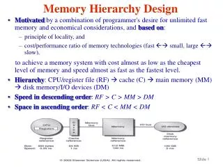
Optimizing Power @ Design Time Memory. Role of Memory in ICs. Memory is very important Focus in this chapter is embedded memory Percentage of area going to memory is increasing. [Ref: V. De, Intel 2006]. Processor Area Becoming Memory Dominated.


Optimizing Power @ Design Time Memory
E N D
Presentation Transcript
Role of Memory in ICs • Memory is very important • Focus in this chapter is embedded memory • Percentage of area going to memory is increasing [Ref: V. De, Intel 2006]
Processor Area Becoming Memory Dominated • On chip SRAM contains 50-90% of total transistor count • Xeon: 48M/110M • Itanium 2: 144M/220M • SRAM is a major source of chip static power dissipation • Dominant in ultra-low power applications • Substantial fraction in others SRAM Intel Penryn™ (Picture courtesy of Intel)
Chapter Outline • Memory Introduction • Power in the Cell Array • Power for Read Access • Power for Write Access • New Memory Technologies
Basic Memory Structures [Ref: J. Rabaey, Prentice’03]
SRAM Metrics Why is functionality a “metric”? • Functionality • Data retention • Readability • Writability • Soft Errors • Area • Power • Process variations increase with scaling • Large number of cells requires analysis of tails (out to 6σ or 7σ) • Within-die VTH variation due to Random Dopant Fluctuations (RDFs)
Where Does SRAM Power Go? • Numerous analytical SRAM power models • Great variety in power breakdowns • Different applications cause different components of power to dominate • Hence: Depends on applications: e.g. high speed versus low power, portable
SRAM cell Three tasks of a cell • Hold data • WL=0; BLs=X • Write • WL=1; BLs driven with new data • Read • WL=1; BLs precharged and left floating BL BL WL Q M3 M6 M2 M5 M4 M1 QB Traditional 6-Transistor (6T) SRAM cell
Key SRAM cell metrics Key functionality metrics • Hold • Static Noise Margin (SNM) • Data retention voltage (DRV • Read • Static Noise Margin (SNM) • Write • Write Margin BL BL WL Q M3 M6 M2 M5 M4 M1 QB Metrics: Area is primary constraint Next: Power, Delay Traditional 6-Transistor (6T) SRAM cell
Static Noise Margin (SNM) BL BLB WL SNM gives a measure of the cell’s stability by quantifying the DC noise required to flip the cell VN M6 M3 M5 M2 QB M1 M4 Q VN Inv 1 Inv 2 0.3 VTC for Inv 2 VTC-1 for Inv 1 VTC for Inv2 with VN = SNM VTC-1 for Inv1 with VN = SNM SNM 0.15 QB(V) SNM is length of side of the largest embedded square on the butterfly curve 0 0.3 0.15 0 Q (V) [Ref: E. Seevinck, JSSC’87]
Static Noise Margin with Scaling Tech and VDD scaling lower SNM • Typical cell SNM deteriorates with scaling • Variations lead to failure from insufficient SNM Variations worsen tail of SNM distribution (Results obtained from simulations with Predictive Technology Models – [Ref: PTM; Y. Cao ‘00])
BLB BL WL 1 1 1 0.8 0.8 0.8 0.6 0.6 0.6 Normalized QB Normalized QB Normalized QB 0 1 1 0 0.4 0.4 0.4 0.2 0.2 0.2 0 0 0 0 0 0 0.2 0.2 0.2 0.4 0.4 0.4 0.6 0.6 0.6 0.8 0.8 0.8 1 1 1 Normalized Q Normalized Q Normalized Q Variability: Write Margin Write failure: Positive SNM Dominant fight (ratioed) Cell stability prior to write: Successful write: Negative “SNM”
VDD=0.6V 0.05 Write Fails 0 -0.05 -0.1 SNM (V) -0.15 TT WW -0.2 SS WS SW -0.25 -40 -20 0 20 40 60 80 100 120 Temperature (oC) Variability: Cell Writability Write margin limits VDD scaling for 6T cells to 600mV, best case. • 65nm process, VDD = 0.6V • Variability and large number of cells makes this worse
Cell Array Power • Leakage Power dominates while the memory holds data BL BL WL Importance of Gate tunneling and GIDL depends on technology and voltages applied ‘1’ ‘0’ Sub-threshold leakage
0.8 -0.2 0 0.2 0.4 0.6 1.0 Using Threshold Voltage to Reduce Leakage • High VTH cells necessary if all else is kept the same • To keep leakage in 1 MB memory within bounds, VTH must be kept in [0.4, 0.6] range 100 Tj=125 C Lg=0.1 m W (QT)=0.20 m W (QD)=0.28 m W (QL)=0.18 m 100 C 75 C 50 C 25 C 10-2 high speed (0.49) 1-Mb array retention current (A) 10-4 low power (0.71) 10 A 10-6 0.1 A 10-8 Average extrapolated VTH(V) at 25 ºC Extrapolated VTH=VTH(nA/m)+0.3 V [Ref: K. Itoh, ISCAS’06]
BL BL BL BL WL WL Multiple Threshold Voltages ‘0’ Dual VTH cells with low VTHaccess transistors provide good tradeoffs in power and delay Use high VTHdevices to lower leakage for stored ‘0’, which is much more common than a stored ‘1’ [Ref: Hamzaoglu, et al., TVLSI’02] High VTH Low VTH [Ref: N. Azizi, TVLSI’03]
Multiple Voltages • Selective usage of multiple voltages in cell array • e.g. 16 fA/cell at 25oC in 0.13 μm technology • High VTH to lower sub-VTH leakage • Raised source, raised VDD, and lower BL reduce gate stress while maintaining SNM 1.0V WL=0V 1.0V 1.5V 0.5V [Ref: K. Osada, JSSC’03]
Power Breakdown During Read VDD_Prech • Accessing correct cell • Decoders, WL drivers • For Lower Power: • hierarchical WLs • pulsed decoders • Performing read • Charge and discharge large BL capacitance • For Lower Power : WL Address Mem Cell Sense Amp Data
Hierarchical Word-line Architecture • Reduces amount of switched capacitance • Saves power and lowers delay [Ref’s: Rabaey, Prentice’03; T. Hirose, JSSC’90]
Hierarchical Bitlines • Divide up bitlines hierarchically • Many variants possible • Reduce RC delay, also decrease CV2 power • Lower BL leakage seen by accessed cell Local BLs Global BLs
“1” Bit-line “0” “0” BL Leakage During Read Access • Leakage into non-accessed cells • Raises power and delay • Affects BL differential
Bitline Leakage Solutions VSSWL VSSWL • Hierarchical BLs • Raise VSS in cell • Negative WL voltage • Longer access FETs • Alternative bit-cells • Active compensation • Lower BL precharge voltage “1” “0” “1” “0” VGND Vg Negative Wordline (NWL) Raise VSS in cell (VGND) [Ref: A. Agarwal, JSSC’03]
Lower Precharge Voltage Lower BL precharge voltage decreases power and improves Read SNM • Internal bit-cell node rises less • Sharp limit due to accidental cell writing if access FET pulls internal ‘1’ low
VDDScaling • Lower VDD (and other voltages) via classic voltage scaling • Saves power • Increases delay • Limited by lost margin (read and write) • Recover Read SNM with read assist • Lower BL precharge • Boosted cell VDD[Ref: Bhavnagarwala’04, Zhang’06] • Pulsed WL and/or Write-After-Read [Ref: Khellah’06] • Lower WL [Ref: Ohbayashi’06]
Power Breakdown During Write VDD_Prech • Accessing cell • Similar to Read • For Lower Power: • Hierarchical WLs • Performing write • Traditionally drive BLs full swing • For Lower Power : • Charge sharing • Data dependencies • Low swing BLs with amplification WL Address Mem Cell Data
Charge recycling to reduce write power • Share charge between BLs or pairs of BLs • Saves for consecutive write operations • Need to assess overhead Basic charge recycling – saves 50% power in theory 1 0 1 BL= 0V BLB= VDD BL= VDD/2 BLB= VDD/2 BL= VDD BLB= 0V old values connect floating BLs disconnect and drive new values [Ref’s: K. Mai, JSSC’98; G. Ming, ASICON’05]
Memory Statistics • 0’s more common • SPEC2000: 90% 0s in data • SPEC2000: 85% 0s in instructions • Assumed write value using inverted data as necessary [Ref: Y. Chang, ISLPED’99] • New Bitcell: BL WZ BL WL WWL 1R, 1W port W0: WZ=0, WWL=1, WS=1 W1: WZ=1, WWL=1, WS=0 WS [Ref: Y. Chang, TVLSI’04]
Low-Swing Write • Drive the BLs with low swing • Use amplification in cell to restore values VDD_Prech EQ BL BLB SLC WL WL Q QB EQ SLC WE VWR=VDD-VTH-delVBL column decoder VWR BL/BLB VDD-VTH-delVBL Din VDD-VTH Q/QB WE [Ref: K. Kanda, JSSC’04]
Write Margin • Fundamental limit to most power-reducing techniques • Recover write margin with write assist, e.g. • Boosted WL • Collapsed cell VDD[Itoh’96, Bhavnagarwala’04] • Raised cell VSS[Yamaoka’04, Kanda’04] • Cell with amplification [Kanda ’04]
Non-traditional cells • Key tradeoff is with functional robustness • Use alternative cell to improve robustness, then trade off for power savings • e.g. Remove read SNM • Register file cell • 1R, 1W port • Read SNM eliminated • Allows lower VDD • 30% area overhead • Robust layout RWL WBL WBL WWL RBL 8T SRAM cell [Ref: L. Chang, VLSI’05]
Cellss with Pseudo-Static SNM Removal • Isolate stored data during read • Dynamic storage for duration of read BL BL WL BL BL WL WWL WLW WLB Differential read Single-ended read [Ref: K. Takeda, JSSC’06] [Ref: S. Kosonocky, ISCICT’06]
Emerging Devices: Double-gate MOSFET • Emerging devices allow new SRAM structures • Back-gate biasing of thin-body MOSFET provides improved control of short-channel effects, and re-instates effective dynamic control of VTH. Gate length = Lg Gate length = Lg Source Gate Source Gate2 VTHControl Fin Width = TSi Gate1 Drain Drain Fin Height HFIN = W Switching Gate Fin Height HFIN = W/2 • Back-gated (BG) MOSFET • Independent front and back gates • One switching gate and VTHcontrol gate Double-gated (DG) MOSFET [Ref: Z. Guo, ISLPED’05]
6T SRAM Cell with Feed-back • Double-Gated (DG) NMOS pull-down and PMOS load devices. • Back-Gated (BG) NMOS access devices dynamically increase β-ratio. • SNM during read ~ 300mV. • Area penalty ~ 19% 6T DG-MOS 6T BG-MOS [Ref: Z. Guo, ISLPED’05]
Summary and Perspectives • Functionality is main constraint in SRAM • Variation makes the outlying cells limiters • Look at hold, read, write modes • Use various methods to improve robustness, then trade off for power savings • Cell voltages, thresholds • Novel bit-cells • Emerging devices • Embedded memory major threat to continued technology scaling – innovative solutions necessary
References Books and Book Chapters • K. Itoh et al, Ultra-Low Voltage Nano-scale Memories, Springer 2007. • A. Macii, “Memory Organization for Low-Energy Embedded Systems,” in Low-Power Electronics Design, C, Piguet Editor, Chapter 26, CRC Press, 2005. • V. Moshnyaga and K. Inoue, “Low Power Cache Design,” in Low-Power Electronics Design, C, Piguet Editor, Chapter 25, CRC Press, 2005. • J. Rabaey, A. Chandrakasan, and B. Nikolic, Digital Integrated Circuits, 2003. • T. Takahawara and K. Itoh, “Memory Leakage Reduction,” in Leakage in Nanometer CMOS Technologies, S. Narendra, Ed, Chapter 7, Springer 2006. Articles • A. Agarwal, H. Li, and K. Roy, “A Single-Vt Low-Leakage Gated-Ground Cache for Deep Submicron,” IEEE Journal of Solid-State Circuits, vol. 38, no. 2, pp. 319–328, Feb. 2003. • N. Azizi, F. Najm, and A. Moshovos, “Low-leakage Asymmetric-Cell SRAM,” IEEE Transactions on VLSI, vol. 11, no. 4, pp. 701-715, August 2003. • A. Bhavnagarwala, S. Kosonocky, S. Kowalczyk, R. Joshi, Y. Chan, U. Srinivasan, and J. Wadhwa, “A Transregional CMOS SRAM with Single, Logic VDD and Dynamic Power Rails,” in Symposium on VLSI Circuits, pp. 292–293, 2004. • Y. Cao, T. Sato, D. Sylvester, M. Orshansky, and C. Hu, “New Paradigm of Predictive MOSFET and Interconnect Modeling for Early Circuit Design,” in Custom Integrated Circuits Conference (CICC), Oct. 2000, pp. 201–204. • L. Chang, D. Fried, J. Hergenrother, et al., “Stable SRAM cell design for the 32 nm node and beyond,” Symposium on VLSI Technology, pp. 128-129, June 2005. • Y. Chang, B. Park, and C. Kyung, “Conforming inverted data store for low power memory,” IEEE International Symposium on Low Power Electronics and Design, 1999.
References (cntd) • Y. Chang, F. Lai, and C. Yang, “Zero-aware asymmetric SRAM cell for reducing cache power in writing zero,” IEEE Transactions on VLSI Systems, vol. 12, no. 8, pp. 827 – 836, August 2004. • Z. Guo, S. Balasubramanian, R. Zlatanovici, T.-J. King, and B. Nikolic, ”FinFET-based SRAM design,” International Symposium onLow Power Electronics and Design, pp. 2-7, August 2005. • F. Hamzaoglu, Y. Ye, A. Keshavarzi, K. Zhang, S. Narendra, S. Borkar, M. Stan, and V. De, “Analysis of Dual-VT SRAM Cells with Full-Swing Single-Ended Bit Line Sensing for On-Chip Cache,” IEEE Transactions on Very Large Scale Integration (VLSI) Systems, vol. 10, no. 2, pp. 91–95, Apr. 2002. • T. Hirose, H. Kuriyama, S. Murakami, et al., IEEE Journal of Solid-State Circuits, vol. 25, no. 5, pp. 1068-1074, October 1990 • K. Itoh, A. Fridi, A. Bellaouar, and M. Elmasry, “A Deep Sub-V, Single Power-Supply SRAM Cell with Multi-VT, Boosted Storage Node and Dynamic Load,” Symposium on VLSI Circuits, pp. 132–133, June 1996. • K. Itoh, M. Horiguchi, and T. Kawahara, “Ultra-low voltage nano-scale embedded RAMs,” IEEE Symposium on Circuits and Systems, May 2006. • K. Kanda, H. Sadaaki, and T. Sakurai, “90% Write Power-Saving SRAM Using Sense-Amplifying Memory Cell,” IEEE Journal of Solid-State Circuits, vol. 39, no. 6, pp. 927–933, June 2004. • S. Kosonocky, A. Bhavnagarwala, and L. Chang, International Conference on Solid-State and Integrated Circuit Technology, pp. 689-692, October 2006. • K. Mai, T. Mori, B. Amrutur, et al., IEEE Journal of Solid-State Circuits, vol. 33, no. 11, pp. 1659-1671, November 1998. • G. Ming, Y. Jun, and X. Jun, "Low Power SRAM Design Using Charge Sharing Technique," pp. 102-105, ASICON, 2005. • K. Osada, Y. Saitoh, E. Ibe, and K. Ishibashi, “16.7-fA/Cell Tunnel-Leakage- Suppressed 16-Mb SRAM for Handling Cosmic-Ray-Induced Multierrors,” IEEE Journal of Solid-State Circuits, vol. 38, no. 11, pp. 1952–1957, Nov. 2003. • PTM – Predictive Models. Available: http://www.eas.asu.edu/˜ptm
References (cntd) E. Seevinck, F. List, and J. Lohstroh, “Static Noise Margin Analysis of MOS SRAM Cells,” IEEE J. of Solid-State Circuits, vol. SC-22, no. 5, pp. 748–754, Oct. 1987. K. Takeda, Y. Hagihara, Y. Aimoto, M. Nomura, Y. Nakazawa, T. Ishii, and H. Kobatake, “A Read-Static-Noise-Margin-Free SRAM Cell for Low-Vdd and High-Speed Applications,” in IEEE International Solid-State Circuits Conference, pp. 478–479, February 2005. M. Yamaoka, Y. Shinozaki, N. Maeda, Y. Shimazaki, K. Kato, S. Shimada, K. Yanagisawa, and K. Osadal, “A 300MHz 25μA/Mb Leakage On-Chip SRAM Module Featuring Process-Variation Immunity and Low-Leakage-Active Mode for Mobile-Phone Application Processor,” in IEEE International Solid-State Circuits Conference, 2004, pp. 494–495.