Download
1 / 10
100 likes | 181 Views
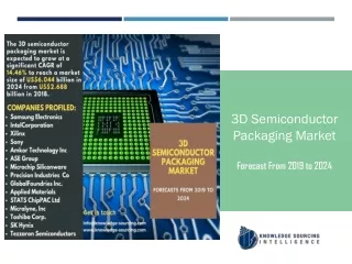
Increase in trend of miniaturization in portable electronic industry and rise in dependency on these devices worldwide is shifting device manufacturers toward finding new methods of size reduction and overall efficiency enhancement of these devices, thus driving the growth of 3D semiconductor packaging market

E N D
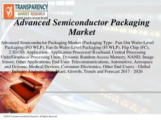
World 3D Semiconductor Packaging Market Opportunities and Forecasts, 2014 – 2022 Published Date: 29-Dec-16
3D semiconductor packaging is an advanced packaging technology to fabricate high-performance chips such as flash memories, DRAMS, NAND, and others, which are highly used in high-performance computers, image sensors, smartphones, and others. • The demand for 3D semiconductor packaging market is globally expected to rise during the forecast period due to increase in demand for miniaturized circuits and short replacement period of electronics products • Surge in the automotive sector and growth in demand for miniature circuits in portable electronic devices provide opportunities in the market. Asia-Pacific dominated the market in 2015, accounting over 50% of the total market revenue, and is expected to maintain its dominance throughout the forecast period. • 3D SEMICONDUCTOR PACKAGING MARKET - INTRODUCTION
3D SEMICONDUCTOR PACKAGINGMARKET - KEY FINDINGS • 3D wire bonded dominated the market in 2015 with over 43% of market share, however, 3D TSV is expected to witness the highest growth rate of 17% In 2015, • Die attach materials is estimated to be one of the fastest growing segment in coming years, growing at an estimated CAGR of 17.4%, • Asia-Pacific dominated the market in 2015, countries such as China, South Korea and Japan supported the growth in the region • In North America, United States accounts for over 70% of the overall market owing to high penetration of 3D TSV technology.
TABLE OF CONTENTS • INTRODUCTION • EXECUTIVE SUMMARY • MARKET OVERVIEW • GLOBAL 3D SEMICONDUCTOR PACKAGING MARKET, BY TECHNOLOGY • GLOBAL 3D SEMICONDUCTOR PACKAGING MARKET, BY MATERIAL • WORLD 3D SEMICONDUCTOR PACKAGING MARKET, BY GEOGRAPHY • COMPANY PROFILES
3D SEMICONDUCTOR PACKAGING MARKET - BY GEOGRAPHY North America, Europe, Asia Pacific, LAMEA
COMPANYPROFILES Amkor Technology ASE group Siliconware Precision Industries Co. Jiangsu Changjiang Electronics Technology Co. SSS MicroTec AG., International Business Machines Corporation (IBM) Intel Corporation Qualcomm Technologies STMicroelectronics Taiwan Semiconductor Manufacturing Company
THANK YOU Thank You! For More Details Visit us at https://www.alliedmarketresearch.com/3D-semiconductor-packaging-market Follow Us On