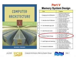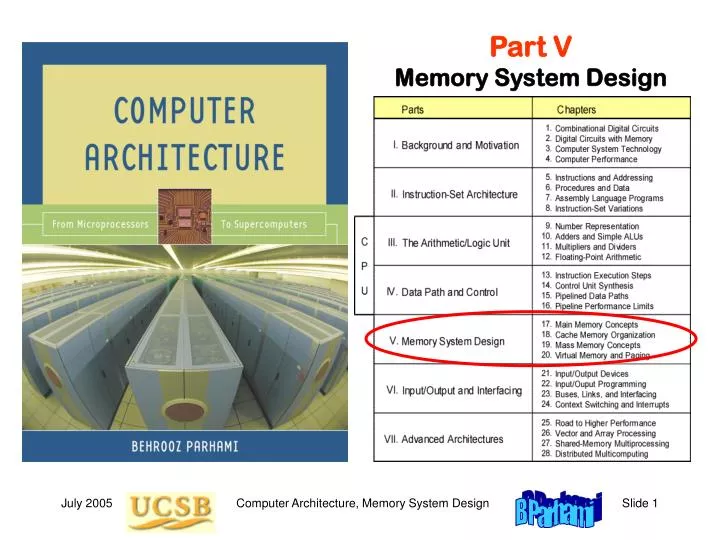

Part V Memory System Design
E N D
Presentation Transcript
Part VMemory System Design Computer Architecture, Memory System Design
V Memory System Design • Design problem – We want a memory unit that: • Can keep up with the CPU’s processing speed • Has enough capacity for programs and data • Is inexpensive, reliable, and energy-efficient Computer Architecture, Memory System Design
17 Main Memory Concepts • Technologies & organizations for computer’s main memory • SRAM (cache), DRAM (main), and flash (nonvolatile) • Interleaving & pipelining to get around “memory wall” Computer Architecture, Memory System Design
17.1 Memory Structure and SRAM Fig. 17.1 Conceptual inner structure of a 2hg SRAM chip and its shorthand representation. Computer Architecture, Memory System Design
Multiple-Chip SRAM Fig. 17.2 Eight 128K 8 SRAM chips forming a 256K 32 memory unit. Computer Architecture, Memory System Design
SRAM with Bidirectional Data Bus Fig. 17.3 When data input and output of an SRAM chip are shared or connected to a bidirectional data bus, output must be disabled during write operations. Computer Architecture, Memory System Design
17.2 DRAM and Refresh Cycles DRAM vs. SRAM Memory Cell Complexity gnd gnd Fig. 17.4 Single-transistor DRAM cell, which is considerably simpler than SRAM cell, leads to dense, high-capacity DRAM memory chips. Computer Architecture, Memory System Design
DRAM Refresh Cycles and Refresh Rate Fig. 17.5 Variations in the voltage across a DRAM cell capacitor after writing a 1 and subsequent refresh operations. Computer Architecture, Memory System Design
DRAM Packaging 24-pin dual in-line package (DIP) Fig. 17.6 Typical DRAM package housing a 16M 4 memory. Computer Architecture, Memory System Design
DRAM Evolution Fig. 17.7 Trends in DRAM main memory. Computer Architecture, Memory System Design
17.3 Hitting the Memory Wall Fig. 17.8 Memory density and capacity have grown along with the CPU power and complexity, but memory speed has not kept pace. Computer Architecture, Memory System Design
Bridging the CPU-Memory Speed Gap Idea: Retrieve more data from memory with each access Fig. 17.9 Two ways of using a wide-access memory to bridge the speed gap between the processor and memory. Computer Architecture, Memory System Design
17.4 Pipelined and Interleaved Memory Memory latency may involve other supporting operations besides the physical access itself Virtual-to-physical address translation (Chap 20) Tag comparison to determine cache hit/miss (Chap 18) Fig. 17.10 Pipelined cache memory. Computer Architecture, Memory System Design
Memory Interleaving Fig. 17.11 Interleaved memory is more flexible than wide-access memory in that it can handle multiple independent accesses at once. Computer Architecture, Memory System Design
17.5 Nonvolatile Memory ROM PROM EPROM Fig. 17.12 Read-only memory organization, with the fixed contents shown on the right. Computer Architecture, Memory System Design
Flash Memory Fig. 17.13 EEPROM or Flash memory organization. Each memory cell is built of a floating-gate MOS transistor. Computer Architecture, Memory System Design
17.6 The Need for a Memory Hierarchy The widening speed gap between CPU and main memory Processor operations take of the order of 1 ns Memory access requires 10s or even 100s of ns Memory bandwidth limits the instruction execution rate Each instruction executed involves at least one memory access Hence, a few to 100s of MIPS is the best that can be achieved A fast buffer memory can help bridge the CPU-memory gap The fastest memories are expensive and thus not very large A second (third?) intermediate cache level is thus often used Computer Architecture, Memory System Design
Typical Levels in a Hierarchical Memory Fig. 17.14 Names and key characteristics of levels in a memory hierarchy. Computer Architecture, Memory System Design