Download
1 / 9
90 likes | 191 Views
This report analyzes VDDA syndrome occurrences in two AMS modules (chips 5 and B) connected with mating sensors. Faults appeared near row 32 in specified columns on both chips, with confirmations of debris through optical microscopy. Deposits were found at rows 20 and 21 in chip5 and at row 28 in chipB, posing risks for further VDDA syndrome. Observations using X-ray reveal that the debris may consist of low-Z materials like silicon or diamond. Actions taken include removal of excess material to prevent further damage to pixel pads.

E N D
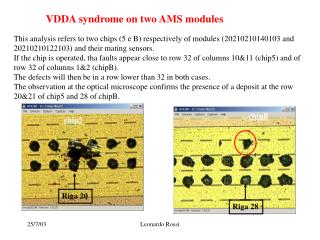
VDDA syndrome on two AMS modules This analysis refers to two chips (5 e B) respectively of modules (20210210140103 and 20210210122103) and their mating sensors. If the chip is operated, tha faults appear close to row 32 of columns 10&11 (chip5) and of row 32 of columns 1&2 (chipB). The defects will then be in a row lower than 32 in both cases. The observation at the optical microscope confirms the presence of a deposit at the row 20&21 of chip5 and 28 of chipB. chipB chip5 Riga 20 Riga 28 Leonardo Rossi
Similar deposits are on the mating (note: all pictures (including the x-rays) are taken with the bumps toward the camera). It is evident that the residue on chip5 is still taller than adjacent bumps and therefore risks to cause another VDDA syndrome in the chip we are going to flip again.. This is also confirmed in the “side view” of the chip (see next page). Leonardo Rossi
Blow-up of chip5, col 10&11, row 21&22 Side view of chip5, col 10&11, row 21&22 Side view of chip5, col 10&11, row 15 (a typical bump pair). Leonardo Rossi
Sensors and chips are then observed at the x-ray mchine to see if the debris is visible (I.e. of high Z). Row 20 chip5 Col 10&11 Leonardo Rossi
Sensor in front of chip5 Row 20 Col 10&11 Leonardo Rossi
chipB Row 28 Col 1&2 Leonardo Rossi
Sensor in front of chip B Row 28 Col 1&2 Leonardo Rossi
I then conclude that the debris is invisible at x-rays and has therefore low Z. The most likely explanation is that it is made out of Silicon of the wafer or Diamond of the blade. Leonardo Rossi
Before sending the module 20210210140103 to be reworked I take out with a manipulator the excess material around [col10&11, row 21&22]. The operation eliminates the exess material but, unavoidably, scratches the pixel pads (row 21, col 10 e col 11). Leonardo Rossi