Download
1 / 24
240 likes | 571 Views
Printed Circuit Board Design Flow CS194-5, Spring 2008 February 4, 2008. Prabal Dutta prabal@cs.berkeley.edu http://www.cs.berkeley.edu/~prabal. Inspiration (Concept) “An air-deployable motion sensor with 10 meter range and 6 month lifetime.”. Implementation (Working System).

E N D
Printed Circuit Board Design Flow CS194-5, Spring 2008 February 4, 2008 Prabal Dutta prabal@cs.berkeley.edu http://www.cs.berkeley.edu/~prabal
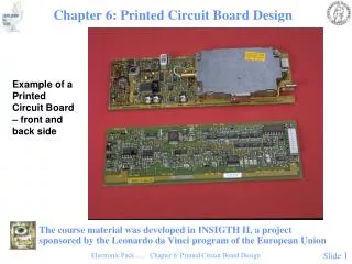
Inspiration (Concept) “An air-deployable motion sensor with 10 meter range and 6 month lifetime.” Implementation (Working System) A design flow is a rough guide for turninga concept into a real, live working system
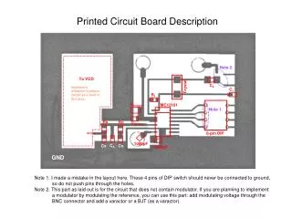
Starting with the end in mind: a printed circuit board Copper (pads & traces) Silkscreen (white) Soldermask (green) Bottom side Top side Drill files (size & x-y coords)
A practical PCB design flow that isaction-oriented and artifact-focused Needs Reqs, Budget, Constraints In library, In stock, Standards Constraints Capability Standards Brainstorm Evaluate* Design (High-level) Capture (Logical Design) Layout (Physical Design) Design concepts (multiple) Figures, Rankings, Tradeoffs Sys arch, block diag ERC/Sim, Sch/Netlist BOM DRC, PCB Files, MFG Files *evaluate through models, prototypes, and discussions
Brainstorming • Goal: generate as many ideas as possible! • Use the “needs” as the rough guide • Do not (yet) be limited by constraints or formal requirements • Ideally, brainstorm in a group so diversity of perspectives emerge
Brainstorming example: energy metering in sensor networks • Need: measure the energy consumed by a mote • Brainstorm • Resulting design concepts • Single-chip battery “fuel gauge” • High-side sense resistor + signal processing • Low-side sense resistor + signal processing • Pulse-frequency modulated switching regulator
Requirements and constraints address the myriadof important details that the system must satisfy • Requirements address: • Functionality • Performance • Usability • Reliability • Maintainability • Budgetary • Requirements may be at odds! • Use correlation matrix to sort things out in this case
Evaluation • Goal: identify best candidates to take forward • Use requirements and constraints as the metric • Get buy-in from stakeholders on decisions • Also consider • Time-to-market • Economics • Non-recurring engineering (NRE) costs • Unit cost • Familiarity • Second-source options • If none of the candidates pass, two options • Go back to brainstorming • Adjust the requirements (hard to change needs though)
Evaluation example: energy metering in sensor networks Requirements: Low High Low High Low CostAccuPowerRezPert. Design concepts Energy meter IC N Y N Y Y High-side sense resistor N Y N Y Y + signal processing Low-side sense resistor Y Y Y Y N + signal processing PFM switching regulator Y Y Y Y Y
Evaluation example: energy metering in sensor networks Accuracy / linearity are really important for an instrument Sometimes a single experiment or figure says a lot
Design • Translate a concept into a block diagram • Translate a block diagram into components • Top-down • Start at a high-level and recursively decompose • Clearly define subsystem functionality • Clearly define subsystem interfaces • Bottom-up • Start with building blocks and increasing integrate • Add “glue logic” between building blocks to create • Combination • Good for complex designs with high-risk subsystems
Design II • Design can be difficult • Many important decisions must be made • Analog or digital sensing? • 3.3V or 5.0V power supply? • Single-chip or discrete parts? • Many tradeoffs must be analyzed • Higher resolution or lower power? • Higher bit-rate or longer range, given the same power? • Decisions may be coupled and far-ranging • One change can ripple through the entire design • Avoid such designs, if possible • Difficult in complex, highly-optimized designs
Schematic capture turns a block diagram into a detail design • Parts selection • In library? • Yes: great, just use it! (BUT VERIFY FIRST!) • No: must create a schematic symbol. • In stock? • Yes: great, can use it! • No: pick a different park (VERIFY LEADTIME) • Under budget? • Right voltage? Beware: 1.8V, 3.3V, 5.0V • Rough floorplanning • Place the parts • Connect the parts • Layout guidelines (e.g. 50 ohm traces, etc.)
Input: schematic (or netlist) Uses: part libraries Outputs Gerbers photoplots (top, bottom, middle layers) Copper Soldermask Silkscreen NC drill files Aperture X-Y locations Manufacturing Drawings Part name & locations Pick & place file Actions Create parts Define board outline Floorplanning Define layers Parts placement Manual routing (ground/supply planes, RF signals, etc.) Auto-routing (non-critical signals) Design rule check (DRC) Layout is the process of transforming a schematic (netlist)into a set of Gerber and drill files suitable for manufacturing
Layout constraints can affect the board size, component placement, and layer selection • Constraints are requirements that limit the design space (this can be a very good thing) • Examples • The humidity sensor must be exposed • The circuit must conform to a given footprint • The system must operate from a 3V power supply • Some constraints are hard to satisfy yet easy to relax…if you communicate well with others. Passive/aggressive is always a bad a idea here! • Advice: the requirement “make it as small as possible” is not a constraint. Rather, it is a recipe for a highly-coupled, painful design.
Layout: board house capabilities, external constraints, and regulatory standards all affect the board layout
Layout tips • Teaching layout is a bit like teaching painting • Suppy/Ground planes • Use a ground plane (or ground pour) if possible • Use a star topology for distributing power • Split analog and digital grounds if needed • Use thick power lines if no supply planes • Place bypass capacitors close to all ICs • Layers • Two is cheap
There are lots of design flows in theliterature but they are awfully general