DOPING
DOPING. “DONATION”. DOPANTS. N type P type ( donor impurities ) ( acceptor impurities ) - antimony - aluminum - arsenic - boron - bismuth - gallium - phosporus - indium. MAJORITY and MINORITY CHARGE CARRIERS.

DOPING
E N D
Presentation Transcript
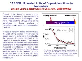
DOPANTS N type P type (donorimpurities) (acceptorimpurities) -antimony -aluminum -arsenic -boron -bismuth -gallium -phosporus -indium
MAJORITY and MINORITY CHARGE CARRIERS Chargecarriers are thosethatinhibitscurrentconduction in a semiconductor which are eitherelectrons (-) orholes (+).
Thedominatingchargecarriers , whetherholesorelectrons, are themajoritycarriers. Thelessabundantones are theminoritycarriers.
ELECTRON FLOW In a N type semiconductor, most of thecurrentflows as “electrons” passingfromatomtoatom. This defines anelectronflow.
HOLE FLOW In a P type semiconductor, most of thecurrentflows as an “electronabsence”. Theabsences, called “holes”, move in a directionoppositetothat of theelectrons. This defines theholeflow.
A resistor mustbeincluded in a circuittopreventdestruction of thediodebytheexcessivecurrent.
FORWARD BREAKOVER VOLTAGE Thisisessentialforconductiontooccur, wherein, itvariesfromabout 0.3V to 1V. Itsapplication can beuseful in amplitudelimiters, waveformclippers and tresholddetectors.
Howdoesjunctionworks? • Forward bias • Reverse bias
JUNCTION CAPACITANCE Some P-N junctions can alternatebetweenconduction (in forward bias) and nonconduction (in reverse bias) millionsorbillions of times per second. Otherjunctions are slower.
Thecapacitanceisthemainlimitting factor at the P-N junctionduringconditions of reverse bias.
Theamount of capacitancedependsonseveralfactors: • Operatingvoltage • Type of semiconductor material • Cross-sectionalarea of the P-N junction
Junction capacitance can bevariedbychangingthe reverse-biasvoltage, becausethevoltageaffectsthewidth of thedepletionregion.
AVALANCE EFFECT “Ifthe reverse biasgoespasttehcriticalvalue of depletion, thevoltageovercomestheability of thejunctiontopreventtheflow of current, and thejunctionconducts as ifitwere forward biased.”
Somecomponents are designedtotakeadvantage of theavalancheeffect. In other cases, avalancheeffectlimitsthe performance of a circuit.