Download
1 / 58
590 likes | 613 Views
ClickNP project aims to make FPGA accessible to software developers for flexible, modularized, and high-performance network function virtualization. It addresses software NF scale-up challenges, latency issues, and FPGA programmability to achieve efficient CPU/FPGA joint packet processing.

E N D
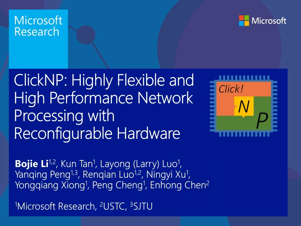
ClickNP: Highly Flexible and High Performance Network Processing with Reconfigurable Hardware Bojie Li1,2, Kun Tan1, Layong (Larry) Luo1, Yanqing Peng1,3, Renqian Luo1,2, Ningyi Xu1, Yongqiang Xiong1, Peng Cheng1, Enhong Chen2 1Microsoft Research, 2USTC, 3SJTU
Virtualized network functions Virtualized NFs on servers to maximize flexibility Dedicated hardware NFs are not flexible NAT LoadBalancer IPSecGateway Firewall LoadBalancerVMs FirewallVMs NATVMs IPSecGatewayVMs
Scale-up challenges for software NF Limited processing capacity Number of CPU cores needed for 40 Gbps line rate
Scale-up challenges for software NF Limited processing capacity Number of CPU cores needed for 40 Gbps line rate Inflated and unstable latency Add tens of microseconds to milliseconds latency to data plane Latency may grow to milliseconds under high load 1 ms occasional delay would violate SLA (e.g., trading services)
FPGA in the cloud FPGA-based SmartNIC Bump-in-the-wire processing betweenNIC and ToR switch[1] [1] SIGCOMM’15 keynote (also the image source)
FPGA in the cloud FPGA-based SmartNIC Bump-in-the-wire processing betweenNIC and ToR switch[1] Why FPGA? Massive parallelism - Millions of logic elements Thousands of “cores” in parallel - Thousands of memory blocks TB/s memory bandwidth Low power consumption (~20W) General computing platform (vs. GPU, NP)to accelerate various cloud services Mature technology with a reasonable price [1] SIGCOMM’15 keynote (also the image source)
FPGA challenge: Programmability Hardware description language (HDL): push many software developers away DMA Engine PCIe Core always @ (posedge SYSCLK or negedge RST_B) begin if(!RST_B) DMA_TX_DATA <= `UD 8'hff; else DMA_TX_DATA <= `UD DMA_TX_DATA_N; end //send: "hello world !" always @ (posedge SYSCLK) begin if (rst) begin dma_data <= 88’h0; dma_valid <= 1’b0; else if (dma_start) begin dma_data <= 88’h68656C6C6F20776F726C64; dma_valid <= 1’b1; end else begin dma_data <= 88’h0; dma_valid <= 1’b0; end end end Ahhhhhhhhhhhh!
Project ClickNP Making FPGA accessible to software developers Flexibility: fully programmable using high-level language Modularized: Click abstractions familiar to software developers; easy code reuse High performance: high throughput; microsecond-scale latency Joint CPU/FPGA packet processing: FPGA is no panacea; fine-grained processing separation
Programming model as if programming on a multi-core processor cores (elements) running in parallel A B C mem mem mem communicate via channels, not shared memory
Element: single-threaded core states (reg/mem) Process handler output channels input channels (main thread) (I/O) (I/O) Signal handler (ISR) signal/control from host (interrupt)
Extension 1: CPU element Write once, run on both FPGA and CPU Compile to a logic block on FPGA or a binary running on CPU Enable joint CPU/FPGA programming Simplify debugging PCIe I/O channel Enable fast communication between elements on FPGA and CPU Low latency: 1 μs High throughput: 25.6 Gbps (PCIe Gen2 x8) Element B(CPU) Element A(FPGA) mem mem PCIe I/Ochannel
Extension 2: Verilog Element Embedding native Verilog code in ClickNP element Enable hybrid C/Verilog programming (analog to C/ASM in CPU world)
Architecture ClickNP host process ClickNP elements Mgrthrd Worker thrd ClickNP host mgr ClickNP library ClickNP script vendor libs PCIe I/O channel Host Catapult PCIe Driver ClickNP compiler Intermediate C files FPGA Catapult shell C compiler vendor HLS ClickNP Verilog vendor specific runtime Cross-platform toolchain Altera OpenCL / Vivado HLS Visual Studio / GCC
Architecture ClickNP host process ClickNP elements Mgrthrd Worker thrd ClickNP host mgr ClickNP library ClickNP script vendor libs PCIe I/O channel Host Catapult PCIe Driver ClickNP compiler Intermediate C files FPGA Catapult shell C compiler vendor HLS ClickNP Verilog vendor specific runtime Cross-platform toolchain Altera OpenCL / Vivado HLS Visual Studio / GCC
Architecture ClickNP host process ClickNP elements Mgrthrd Worker thrd ClickNP host mgr ClickNP library ClickNP script vendor libs PCIe I/O channel Host Catapult PCIe Driver ClickNP compiler Intermediate C files FPGA Catapult shell C compiler vendor HLS ClickNP Verilog vendor specific runtime Cross-platform toolchain Altera OpenCL / Vivado HLS Visual Studio / GCC
Architecture ClickNP host process ClickNP elements Mgrthrd Worker thrd ClickNP host mgr ClickNP library ClickNP script vendor libs PCIe I/O channel Host Catapult PCIe Driver ClickNP compiler Intermediate C files FPGA Catapult shell C compiler vendor HLS ClickNP Verilog vendor specific runtime Cross-platform toolchain Altera OpenCL / Vivado HLS Visual Studio / GCC
Architecture ClickNP host process ClickNP elements Mgrthrd Worker thrd ClickNP host mgr ClickNP library ClickNP script vendor libs PCIe I/O channel Host Catapult PCIe Driver ClickNP compiler Intermediate C files FPGA Catapult shell C compiler vendor HLS ClickNP Verilog vendor specific runtime Cross-platform toolchain Altera OpenCL / Vivado HLS Visual Studio / GCC
Architecture ClickNP host process ClickNP elements Mgrthrd Worker thrd ClickNP host mgr ClickNP library ClickNP script vendor libs PCIe I/O channel Host Catapult PCIe Driver ClickNP compiler Intermediate C files FPGA Catapult shell C compiler vendor HLS ClickNP Verilog vendor specific runtime Cross-platform toolchain Altera OpenCL / Vivado HLS Visual Studio / GCC
Example: Packet logger from_tor Count Tee to_tor FPGA CPU logger ClickNP Configuration:
Example: Packet logger from_tor Count Tee to_tor Count element: FPGA CPU logger ClickNP Configuration:
Parallelizing in FPGA Parallelism across elements Pipeline parallelism Data parallelism Parallelism inside an element Minimize memory dependency Use registers Delayed write Memory scattering Balance pipeline stages Unroll loops Offload slow path to another element
Parallelism across elements Pipeline parallelism Duplicate pipeline to leverage data parallelism e1 e2 e3 e1 e2 e3 demux mux e1 e2 e3
Parallelism inside element (1) Element is synthesized into a pipeline Output Loop s 0 1 2 s 0 1 2 s 0 1 2 s 0 1 2 + + + Input Input pkt s += pkt[0] time s += pkt[1] Input + + Output + s += pkt[2] Output + Input + + + Output + + Input Output s + + Output Input +
Parallelism inside element (2) Principle 1: Minimize memory dependency time Loop Read Write Inc Read input Inc Read Write Read mem Inc Read Write Increment Memory dependency: Read cannot start before last write,because read and write addresses may conflict. Write mem Write out
Parallelism inside element (3) Delayed write to remove read-write dependency Memory read and write can operate in parallel: Read in.addr, Write buf.addr Different memory addresses! Loop Loop Read input Read input N Y in.addr = buf.addr? Read mem Read buf Read mem Write mem Increment Mux Write mem Increment Write out Delayed write: Buffer new data in a register Delay memory write until next read Write buf Write out
Parallelism inside element (4) Principle 2: Balance pipeline stages time Loop Read Cache Cache Output Read DRAM Y Cache Output Read DRAM Hit? Cache Output Read DRAM N Read DRAM DRAM read is an unbalanced pipeline stage. Pipeline is scheduled with a fixed interval to cover the worst-case latency. So throughput is bottlenecked by DRAM read latency. Output
Parallelism inside element (5) Offload slow path to another element Fast path Slow path Original Loop Loop Loop Read Cache Read Cache From fast path Y Y Hit? Read DRAM Hit? N N Read DRAM To slow path From slow path To fast path Output Output
Parallelism inside element (6) Offload slow path to another element time 3 cache hits: Cache Output Output Cache Output Cache 1 cache hit, 1 cache miss, 1 cache hit: Cache Output To fast Output Cache To slow Read DRAM Output Cache
ClickNP element library Throughput: 200 Mpps / 100 Gbps Mean delay: 0.19 us, max delay: 0.8 us Mean LoC: 80, max LoC: 196 Nearly 100 elements 20% re-factored from Click modular router Cover packet parsing, checksum, tunnelencap/decap, crypto, hash tables, prefix matching, packet scheduling, rate limiting…
ClickNP element library Throughput: 200 Mpps / 100 Gbps Mean delay: 0.19 us, max delay: 0.8 us Mean LoC: 80, max LoC: 196 Nearly 100 elements 20% re-factored from Click modular router Cover packet parsing, checksum,encap/decap, hash tables, prefix matching,rate limiting, crypto, packet scheduling…
ClickNP element library Throughput: 200 Mpps / 100 Gbps Mean delay: 0.19 us, max delay: 0.8 us Mean LoC: 80, max LoC: 196 Nearly 100 elements 20% re-factored from Click modular router Cover packet parsing, checksum,encap/decap, hash tables, prefix matching,rate limiting, crypto, packet scheduling…
ClickNP element library Throughput: 200 Mpps / 100 Gbps Mean delay: 0.19 us, max delay: 0.8 us Mean LoC: 80, max LoC: 196 Nearly 100 elements 20% re-factored from Click modular router Cover packet parsing, checksum,encap/decap, hash tables, prefix matching,rate limiting, crypto, packet scheduling…
Sample network functions Each NF takes about one week to develop * ClickNP configuration file
Case study: IPSec gateway (1) Why IPSecdatapath offloading? CPU is the bottleneck for computation intensive processing Even with AES-NI, software AES processing is far from 40 Gbps Currently X86 has no SHA-1 acceleration instructions
Case study: IPSec gateway (1) Why IPSecdatapath offloading? CPU is the bottleneck for computation intensive processing Even with AES-NI, software AES processing is far from 40 Gbps Currently X86 has no SHA-1 acceleration instructions Challenges to FPGA offloading AES • Single AES element throughput is 27.8 Gbps (< 40 Gbps) SHA-1 • Packet payload is split into 64-byte data blocks • Dependency between successive data blocks in a packet • Only 1.07 Gbps if processed sequentially!
Case study: IPSec gateway (2) Solution: Parallelizing in FPGA AES-256-CTR: Leverage data parallelism AES Split Merge AES
Case study: IPSec gateway (2) Solution: Parallelizing in FPGA AES-256-CTR: Leverage data parallelism SHA-1: Leverage packet-level parallelism AES Split Merge AES • Process data blocks from different packets in parallel Reservo pkt 1 Reorder Buffer … scheduler pkt n SHA-1
Case study: IPSec gateway (2) Solution: Parallelizing in FPGA AES-256-CTR: Leverage data parallelism SHA-1: Leverage packet-level parallelism AES Split Merge AES • Process data blocks from different packets in parallel Reservo pkt 1 Reorder Buffer … scheduler pkt n SHA-1
Case study: IPSec gateway (3) Single-tunnel performance
Case study: L4 load balancer (1) Requires per-flow states for many flows 32M concurrent flows in off-chip DRAM 16K flow cache in on-chip BRAM Network in Parser Flow cache Mux DRAM Tunnel encap Nexthop allocation Network out CPU element
Case study: L4 load balancer (1) Requires per-flow states for many flows 32M concurrent flows in off-chip DRAM 16K flow cache in on-chip BRAM Requires complex nexthop allocation policy Nexthop allocation in CPU element: joint CPU/FPGA processing Network in Parser Flow cache Mux DRAM Tunnel encap Nexthop allocation Network out CPU element
Case study: L4 load balancer (2) Performance 10M new flows per second 51Mpps for 8K flows 11Mpps for 32M flows 4us stable latency
Area cost Overhead compared to hand-written Verilog
Area cost Overhead compared to hand-written Verilog
Area cost Overhead compared to hand-written Verilog Area cost will be less of a concern Quickly growing FPGA capacity: 1x (2013), 2.5x (2015), 10x (2018)
Conclusion FPGA in the cloud Fast, general and mature ClickNP: programming hardware as software Highly flexible: Program with high-level language Modular: Click-like abstractions High performance: Utilize massive parallelism in FPGA Joint CPU/FPGA packet processing Start from network processing, but it goes beyond… General framework for programming on FPGA Azure storage, Bing search, machine learning…
Acceleration in host Offloading software NFs to accelerator