Download

1 / 38
390 likes | 777 Views
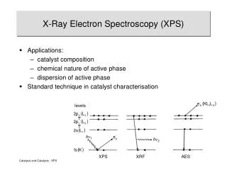
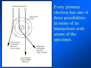
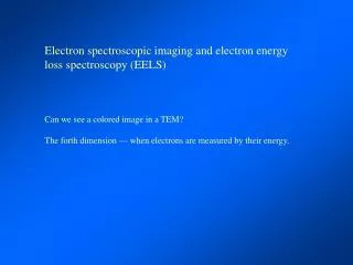
Electron spectroscopic imaging and electron energy loss spectroscopy (EELS) Can we see a colored image in a TEM? The forth dimension --- when electrons are measured by their energy. Every primary electron has one of three possibilities in terms of its interactions with atoms of the specimen.

E N D
Electron spectroscopic imaging and electron energy loss spectroscopy (EELS) Can we see a colored image in a TEM? The forth dimension --- when electrons are measured by their energy.
Every primary electron has one of three possibilities in terms of its interactions with atoms of the specimen.
The energy of a transmitted or elastically scattered electrons, even diffracted ones, remains relatively unchanged. The energy of an inelastically scattered electron is always less than that of the primary electron.
For most of the electrons, the change in energy is not random but is directly related to which electron, from which atom, from which orbital shell the inelastic collision took place.
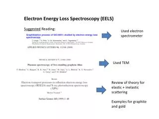
This specific loss of energy is known as Electron Energy Loss Spectroscopy or EELS
One important thing: Unlike x-rays (EDX), an electron beam traversing a thin sample may lose any amount of energy. One good reference: Egerton R F 1996 Electron Energy-Loss Spectroscopy in the Electron Microscope (New York: Plenum)
As in light optics the resultant polychromatic illumination can be broken down based on the wavelength, which in tern, is determined by the energy of the beam.
What a measured EELS spectrum look like? The energy loss spectrum can be displayed and the loss profiles be used to identify elements in a specimen.
EELS Spectra Process of inelastic electron scattering: The Zero-Loss Peak: 1). It is the main feature in EELS spectra of thin specimens. 2). Originates from electrons that have lost NO energy on their way through the specimen (except for small losses due to phonon scattering). 3). Corresponds to undiffracted beam in the diffraction pattern. 4). Width of the zero-loss peak: energy spread of the electron source. 5). Zero loss peak contains less analytical information about the sample. What is phonon? -- Phonons are lattice vibrations, which are equal to heating the specimen. This effect may lead to a damage of the sample.
Low-Loss area: Plasmon 1). It is the region with energy losses up to 50 eV. 2). It reflects excitation of plasmons and interband transitions. What is plasmons: Plasmons are longitudinal oscillations of free electrons, which decay either in photons or phonons. It is caused by weakly bonded or quasi-free electrons. It depends on local density of the weakly bonded electrons. The typical lifetime of plasmons is about 10-15 s. It is localized to about 10 nm and mean free path length for electron scattering (100 keV) at plasmons is about 100 nm. Thin Thick In the EELS spectra, plasmon losses always occur, except the ultra-thin specimens. Thus it can be used to estimate the thickness of the sample. However, when the specimen is quite thick, multiple plasmon losses will make the straightforward analysis impossible. t = p Ln(Ip/I0), p the electron mean free path for plasmon excitation
Low-Loss area: longitudinal oscillations of the valence or conduction band electrons in both the surface and the bulk gives characteristic plasmon energy losses. This energy loss region also contains energy losses from the excitation of inter- and intraband transitions. Band-band transitions: It is the excitation of electrons to an orbital of higher quantum number. Quantitative analysis of the low-loss peak is still difficult. Simplified diagram of band structure of an insulator or semiconductor The low-loss peaks of the Al atoms in different environments. Illustration of inter- and intraband transitions
High-loss Region 1). It is the region with energy losses E > 50 eV. 2). It reflects inelastic scattering in inner regions of atoms, i.e. ionization of inner shells (K, L, M, …). 3). A specific minimum energy, the critical ionization energy EC or ionization threshold, must be transferred from the incident electron to the expelled inner-shell electron, which leads to ionization edges in the spectrum at energy losses that are characteristic for an element. What is ionization? The high-energy electrons of the incident beam can transfer a critical amount of energy to an inner-shell electron of an atom, leading to the ejection of this electron. The ionization energy is provided by the incident electron, reducing its energy. This leads to an ionization edge in the electron energy loss spectrum. The closer a primary electron approaches the nucleus of an atom, the larger can be the energy loss during inelastic scattering. EELS spectrum of BN (boron nitride) Illustration of ionization of inner shells
Why is it ionization (absorption) edge? 1). Electrons should lose at least the energy equal to the critical ionization energy EC for ionization (this energy is the binding energy of the inner-shell electron to the nucleus of atom). 2). At the same time, however, ionization occurs also with larger energy losses: E > Ec. 3). Intensity of the absorption edge decreases with increasing energy loss 4). The edge has a high background. The background is originated from: · multiple inelastic electron scattering · extension of previous absorption edges 5). The most important thing is: from the edge the critical ionization energy Ec can be identified. We then can identify the elements in our sample from the energy.
Like X-ray microanalysis EELS offers a method by which an electron beam’s interaction with the specimen can yield specific information about which elements are present in a specimen.
Two more things about the ionization (absorption) edge. 1. ELNES, “electron loss near-edge structure”: features in the spectrum with energy loss E = Ec to Ec + 50 eV (by definition). It contains information on local density of empty states, oxidation state. 2. EELFS, “extended energy-loss fine structure”: features in the spectrum with energy loss E > Ec + 50 eV. It contains information on local coordination of the respective atom. multiple inelastic scattering · ionization followed by plasmon scattering; modulation at Ec + 15..25 eV
Diamond, graphite and fullerene all consist of only carbon. All of these specimens have absorption peaks around 284 eV in EELS corresponding to the existence of carbon atoms. From the fine structure of the absorption peak, the difference in bonding state and local electronic state can be detected. The sharp peak at absorption edge corresponds to the excitation of carbon K-shell electron (1s electron) to empty anti-bonding pi-orbital. It is not observed for diamond, because of no pi-electron in it. eels.kuicr.kyoto-u.ac.jp/eels.en.html
Comparisons of EELS and EDS(X-ray Energy-Dispersive Spectrometer) 1). EELS has higher spatial resolution than EDS. EDAX may be affected by backscattering electron, And fast secondary electron within the sample. 2). EELS has higher energy resolution than EDS. (around 1 eV) 3). EELS is better in detecting light element. 4). EELS contains information of electronic structure. 5). EDS is easy to operate and quick for a qualitative composition analysis. However, EELS Spectra from thick specimens (>50nm) may be difficult to interpret because of plural scattering. Interpretation of fine structure sometimes requires sophisticated calculations.
Electron Spectroscopic Imaging (ESI)It is a contrast-enhancement technique. It improves contrast in images and diffraction patterns by removing inelastically scattered electrons that produce heavy background.It is a mapping technique. It creates elemental (chemical) maps by forming images with inelastically scattered electrons.It is an analytical technique. It records electron energy-loss spectra (and maps) to provide precise chemical analysis of the samples.
When a monochromatic electron beam interacts with a specimen it becomes polychromatic due to multiple scattering events.
An electromagnetic prism is needed to separate the resultant wavelengths. After bouncing off of an electrostatic mirror the selected wavelength of electrons is used to produce an image of the specimen.
Zero-loss images are those created by only using the transmitted, and thus no energy loss, electrons. They have increased contrast due to the elimination of scattered electrons but retain high resolution because an objective lens aperture is not needed to eliminate scattered electrons.
Zero-loss image of a 1.0 mm thick section at 100KeV Multiple scattering events are the primary reason why thick sections cannot normally be imaged in conventional TEM. Zero-loss imaging allows for imaging of thick sections.
Muscle cell Fibroblast Stereo-pair images from thick sections imaged with zero-loss imaging.
Cryoimage of cationic vesicles Increased contrast from low contrast images such as unstained sections or cryo-samples.
Energy filtering can also be used to improve diffraction patterns eliminating scattered, but not diffracted, electrons from the image. Like transmitted electrons diffracted electrons have no energy loss.
One can create an image using only those electrons that were slowed down by their interactions with a specific element. Electron Spectroscopic Imaging or ESI
ESI is usually accomplished by increasing the accelerating voltage of the TEM by precisely the additional energy needed (e.g. 100,250 eV vs. 100,000 eV).
Conventional image Same sample imaged with electrons that have lost 250eV corresponding to Fe
Element specific images can be created but these are not maps because they are not made scanning the beam or collecting the signal as is done with an X-ray map.
High resolution elemental distribution imaging using elemental spectroscopic imaging (ESI) is an optimal complement to high resolution imaging. It provides important additional information about specimen structures. This highly sensitive and fast imaging method can show element demarcations and element distributions with a resolution in the nanometer range within minutes.
Because EELS is not dependent on signal collection even light elements such as Boron can be imaged.
LEO Omega system uses four prisms and no electrostatic mirrors.
The Gatan Imaging Filter (GIF) is an add-on device that can be attached to any TEM. Like the in-column prisms it can separate the signal based on changes in wavelength (energy) and use the results for either EELS or ESI.
At $200K+ the GIF is not for every lab and it occupies the port normally used for high resolution digital cameras.
Advantages of EELS, ESI, and Zero-loss imaging: Elemental Analysis Elemental Imaging and Mapping Improved contrast without loss of resolution Thick specimen imaging Disadvantages: Elemental analysis requires very thin specimens (10-20nm) Mucho $$$ (LEO TEM or GIF on a STEM)
Atomic & Electronic Structure Atomic Diameter Electron Probe y • STEM + EELS makes essential connection between physical & electronic structure, both at atomic resolution x Annular Dark Field (ADF) detector Increasing energy loss Electron Energy Loss Spectrometer