Download
1 / 3
30 likes | 152 Views
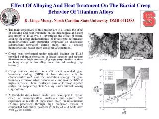
Epit ax i a l VO 2 /TiO 2 hete ro structure Integrated with Sapphire and Si(100) Substrates f o r multifunct io n a l a pp l ic a ti o ns Jagdish Narayan, North Carolina State University, DMR 0803663.

E N D
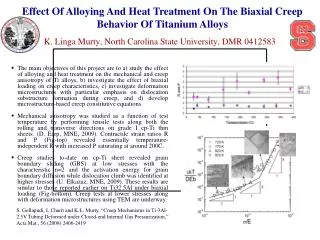
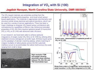
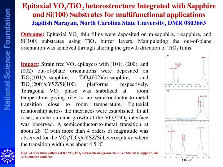
EpitaxialVO2/TiO2heterostructureIntegrated with Sapphire and Si(100) Substrates formultifunctionalapplicationsJagdish Narayan, North Carolina State University, DMR 0803663 Outcome:Epitaxial VO2 thin films were deposited on m-sapphire, r-sapphire, and Si(100) substrates using TiO2 buffer layers. Manipulating the out-of-plane orientation was achieved through altering the growth direction of TiO2 films. Impact:Strain free VO2 epilayers with (101), (200), and (002) out-of-plane orientations were deposited on TiO2(101)/r-sapphire, TiO2(002)/m-sapphire, and TiO2(200)/cYSZ/Si(100) platforms, respectively. Tetragonal VO2 phase was stabilized at room temperature giving rise to an semiconductor-to-metal transition close to room temperature. Epitaxial relationship across the interfaces were established. In all cases, a cube-on-cube growth at the VO2/TiO2 interface was observed. A semiconductor-to-metal transition at about 28 oC with more than 4 orders of magnitude was observed for the VO2/TiO2/cYSZ/Si heteroepitaxy where the transition width was about 4.5 oC. Fig.1. 2Theta/Theta patterns of the VO2/TiO2 heteroepitaxies grown on: (a) YSZ/Si, (b) m-sapphire, and (c) r-sapphire platforms.
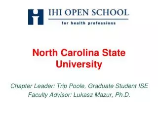
EpitaxialVO2/TiO2heterostructure Integrated with Sapphire and Si(100) Substrates formultifunctionalapplicationsJagdish Narayan, North Carolina State University, DMR 0803663 Growth of high quality epitaxial VO2 films with low mosaicity is confirmed by the phi-scan patterns Fig.2. Phi patterns of the VO2/TiO2 heteroepitaxies grown on: (a) m-sapphire and (b) r-sapphire substrates.
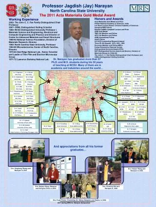
Educational Activities and OutreachJagdish Narayan, North Carolina State University, DMR 0903663 In less than three years, this program has graduated two very successfully employed PhDs, trained four undergraduates, and over fifteen papers in archival journals and equal number in conference proceedings, in addition to 2010 MRS Best Paper Award and several invited talks. Under PI’s leadership, NCSU launched M.S. degree course in Nanoengineering, where students from all over the world including minority (NCA&T and Shaw) institutions, can finish their degree, held very popular ASM Camp for high-school seniors, and transferred technology to Kopin Corporation. PI has also received 2012 Holladay Medal for pioneering contributions in research, teaching and extension, this is a highest faculty honor at NCSU. The MS&T 2011 International Symposium on Advances in nanostructured Materials and Applications (October 16-21, 2011, Columbus, Ohio) was dedicated to Professor Jay Narayan, The John Fan Family Distinguished Chair Professor, N C State University http://www.mse.ncsu.edu/profile/narayan