Download
1 / 14
170 likes | 550 Views
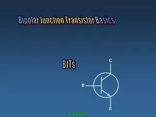
Chapter 10. Bipolar junction transistor fundamentals. Invented in 1948 by Bardeen, Brattain and Shockley Contains three adjoining, alternately doped semiconductor regions: Emitter (E), Base (B), and Collector (C)

E N D
Chapter 10. Bipolar junction transistor fundamentals • Invented in 1948 by Bardeen, Brattain and Shockley • Contains three adjoining, alternately doped semiconductor regions: Emitter (E), Base (B), and Collector (C) • The middle region, base, is very thin compared to the diffusion length of minority carriers • Two kinds: npn and pnp
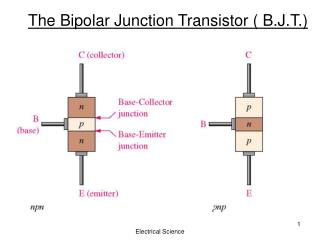
Schematic representation of pnp and npn BJTs Emitter is heavily doped compared to collector. So, emitter and collector are not interchangeable. The base width is small compared to the minority carrier diffusion length. If the base is much larger, then this will behave like back-to-back diodes.
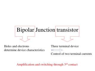
BJT circuit symbols IE = IB + IC and VEB + VBC + VCE = 0 VCE = VEC As shown, the currents are positive quantities when the transistor is operated in forward active mode.
Cross sections and simplified models of discrete and IC npn BJTs
Electrostatic variables for a pnp BJT at equilibrium = charge density = Ks o
Qualitative discussions of operation Consider two diodes, one forward biased and one reverse biased. reverse forward
Qualitative discussion of transistor action Combine the two diodes! VF VR No transistor action
Consider very thin base width: Transistor action E(P+) B(N) C(P) Hole concentration is zero here, reverse biased VF VR The collector current IC is almost equal to IE, and collector current is controlled by the E-B junction bias. The loss, i.e. < 1 corresponds to the recombination of holes in base.
IEP IBR –IEN –IBE –IBR Electron flux Hole flux and current PNP under forward active mode P N P E B C IE =IEP + IEN = 1 + 2 + 5 IB = IBR + IBE = IBR + IEN = – (4 + 5) IC = IEP – IBR= 2
Current components 1 = hole current lost due to recombination in base, IBR 2 = hole current collected by collector, ~ IC 1 + 2 = hole part of emitter current, IEP 5 = electrons injected across forward biased E-B junction, (– IBE); same as electron part of emitter current, – IEN 4 = electron supplied by base contact for recombination with holes lost, – IBR (= 1) 3 = thermally generated e & h making up reverse saturation current of reverse biased C-B junction. (generally neglected)
Performance parameters (Consider pnp) Neglect the reverse leakage (electron) current of C-B junction Emitter efficiency: Fraction of emitter current carried by holes. We want close to 1. Base transport factor: Fraction of holes collected by the collector. We want T close to 1. Common base dc current gain: Note that is less than 1.0 but close to 1.0 (e.g. = 0.99)
Performance parameters (Consider pnp) Common emitter dc current gain, dc: But, Note that is large (e.g. = 100) For npn transistor, similar analysis can be carried out. However, the emitter current is mainly carried by electrons. Example: