آنالیز مدارهای الکترونیکی با استفاده از PSPICE
آنالیز مدارهای الکترونیکی با استفاده از PSPICE. ( OrCAD 9.2). مدرس: بهزاد بهنام Email: b_behnam@kiau.ac.ir 1388/1 2 /1. Introduction PSpice . PSPICE (Personal Simulation Program With Integrated Circuit Emphasis) برنامه شبیه سازی با تاکید بر روی مدارات مجتمع


آنالیز مدارهای الکترونیکی با استفاده از PSPICE
E N D
Presentation Transcript
آنالیز مدارهای الکترونیکی با استفاده ازPSPICE (OrCAD 9.2) مدرس: بهزاد بهنام Email: b_behnam@kiau.ac.ir 1388/12/1 b_behnam@kiau.ac.ir
Introduction PSpice • PSPICE (Personal Simulation Program With Integrated Circuit Emphasis) • برنامه شبیه سازی با تاکید بر روی مدارات مجتمع • PSpice is a simulation program that models the behavior of a circuit. • PSpice simulates analog-only circuits, whereas PSpice A/D simulates any mix of analog and digital devices. b_behnam@kiau.ac.ir
Introduction PSpice • Used with OrCAD Capture for design entry, you can think of PSpice as a software-based breadboard of your circuit that you can use to test and refine your design before manufacturing the physical circuit board or IC. b_behnam@kiau.ac.ir
نحوه نصب ORCAD 9.2 Orcad 9.2 • Run the setup program. • These are the key codes : 1000-00000-0000 for Capture 2000-00000-0000 for Capture CIS 5000-00000-0000 for Layout 6000-00000-0000 for Layout Plus 7000-00000-0000 for Layout Engineer's Edition 8000-00000-0000 for PsPice 9000-00000-0000 for PsPice A/D b_behnam@kiau.ac.ir
نحوه نصب ORCAD 9.2 This is authorization code: 0000-000-0000-00000-00000 b_behnam@kiau.ac.ir
نحوه نصب ORCAD 9.2 2) Run three Orcad Web Updates from the folders : a) \ORCAD92\Orcad web Update\Capture92_WebUpdate1 b) \ORCAD92\Orcad web Update\Capture92_WebUpdate2 c) \ORCAD92\Orcad web Update\Capture92_WebUpdate3 b_behnam@kiau.ac.ir
نحوه نصب ORCAD 9.2 3) Copy the file \ORCAD92\orcadfnc.dll to the three folders (you should overwrite it) : a) C:\Program Files\Orcad\Capture b) C:\Program Files\Orcad\Layout_Plus (or Layout) c) C:\Program Files\Orcad\PSpice b_behnam@kiau.ac.ir
نحوه نصب ORCAD 9.2 4) Copy the file Orcad.lic (with size 0) to the four folders : a) C:\Program Files\Orcad b) C:\Program Files\Orcad\Capture c) C:\Program Files\Orcad\Layout_Plus (or Layout) d) C:\Program Files\Orcad\PSpice b_behnam@kiau.ac.ir
Numeric value conventions Name b_behnam@kiau.ac.ir
Select Capture OR Capture CIS b_behnam@kiau.ac.ir
Funcionalidades de la placa: Se trata del diseño de una placa que ha de hacer de ‘buffer’ para 12 señales que vienen de dos encoders. También se aprovecha para interconectar otros elementos necesarios y proporciona un interfaz con el usuario mediante el uso de unos interruptores y LEDs. b_behnam@kiau.ac.ir
Creating the New Project b_behnam@kiau.ac.ir
Select Analog or Mixed A/D b_behnam@kiau.ac.ir
Select a blank project b_behnam@kiau.ac.ir
For insert component For place wire For insert net alias For insert GND b_behnam@kiau.ac.ir
Placing Parts b_behnam@kiau.ac.ir
Selection component List of libraries That install b_behnam@kiau.ac.ir
Placing Ground • •To place the ground parts (0), click the GND button on the tool palette • •If 0 –ground is absent • Add the library for the parts you need to place: • Click the add library button • Select SOURCE.OLB (from the PSpice library) and • Click open • •Place the ground parts b_behnam@kiau.ac.ir
Editing Parts • Rotation: [R] • Flip horizontally: [H] • Flip vertically: [V] • Double click every property to change b_behnam@kiau.ac.ir
Editing Parts • Double click every part to see and edit full table of properties لطفا به این انتخاب توجه کنید b_behnam@kiau.ac.ir
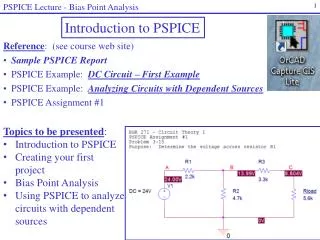
Simulation Types • •Bias point • •DC sweep –sweep of the parameter • •Time domain (transient) • •Frequency domain (AC/Noise) • Additional (multi-run analyses) • •Parametric • •Temperature • Optimization • Monte carlo/Worst case b_behnam@kiau.ac.ir
Simulation Types (DC) Bias-point 1- تمامی منابع مستقل Acبی اثر می شوند. 2- تمامی خازن ها اتصال باز می شوند اما شرایط اولیه آنها بصورت یک منبع ولتاژ در سیستم وارد میشود. 3- تمامی سلف ها اتصال باز می شوند اما شرایط اولیه آنها به صورت یک منبع جریان ظاهر میشوند. 4- در واقع محاسبات جریان و ولتاژ با در نظر گرفتن شرایط اولیه المانهای ذخیره کننده انرژی در زمان t=0 انجام میگیرد. b_behnam@kiau.ac.ir
Simulation Types (DC) Bias-point TOOL b_behnam@kiau.ac.ir
Simulation Types (DC) Simulation Settings (Bias Point) b_behnam@kiau.ac.ir
Simulation Types (DC) Bias-point سئوالات 1- آیا مقدار ظرفیت خازن در نتیجه محاسبات Bias-point تاثیر دارد چرا؟ 2- آیا مقدار ولتاژ اولیه شارژ شده در خازن در نتیجه محاسبات Bias-point تاثیر دارد چرا؟ b_behnam@kiau.ac.ir
Example1: bias point with and without Initial condition voltage in capacitor b_behnam@kiau.ac.ir
Example2: bias point with and without Initial condition current in inductor b_behnam@kiau.ac.ir
Type Names of Elements in BREAKOUT library b_behnam@kiau.ac.ir
Select Dbreak from in BREAKOUT library Dbreak is a diode model that user can modifiy diode parameter b_behnam@kiau.ac.ir
Pspice diode model SPICE diode model with reverse-biased condition. SPICE small-signal diode model. Static diode model with reverse-based condition. b_behnam@kiau.ac.ir
Parameters of Diode Model b_behnam@kiau.ac.ir
DIODE STATEMENT .MODEL SWITCH D(IS=100E–15 CJO=2PF TT=12NS BV=100 IBV=10E–3) b_behnam@kiau.ac.ir
Example3: bias point for diode b_behnam@kiau.ac.ir
.OP (OPERATING POINT) مدار های الکتریکی و الکترونیکی شامل اجزا غیر خطی می باشند (مثل دیود و ترانزیستورها) که پارامتر های سیگنال کوچک آنها وابستگی به نقطه کار Dc آن المان دارد. توجه کنید که نقطه کار همان operating point و bias point quiescent point می باشد. در تمامی محاسبات Pspice ابتدا نقطه کار بدست می آید و سپس در حول نقطه کار مدل خطی المان غیر خطی محاسبه می شود به عبارت دیگر مدل سیگنال کوچک المان غیر خطی محاسبه میشود. دستور .OP در آنالیز bias point علاوه بر محاسبه ولتاژها و جریان های گره ها و شاخه ها محاسبات سیگنال کوچک را برای المان غیر خطی نیز انجام میدهد وآنها بصورت یک فایل متنی در بخش simulation output file قابل مشاهده میباشد. b_behnam@kiau.ac.ir
Example4: .OP for diode .MODEL DX D(IS=100E–15 CJO=2PF TT=12NS BV=100 IBV=10E–3) b_behnam@kiau.ac.ir
Example4: .OP for diode b_behnam@kiau.ac.ir
**** 10/06/09 10:36:30 ********* PSpice 9.2 (Mar 2000) ******** ID# 0 ******** ** Profile: "SCHEMATIC1-diode_bias" [ C:\DOCUMENTS AND SETTINGS\BEHZAD\DESKTOP\BEHZAD\ORCAD_EBOOKS\PPT FOR CLASS\ex_3\diode_bias-SC **** CIRCUIT DESCRIPTION ****************************************************************************** ** Creating circuit file "diode_bias-SCHEMATIC1-diode_bias.sim.cir" ** WARNING: THIS AUTOMATICALLY GENERATED FILE MAY BE OVERWRITTEN BY SUBSEQUENT SIMULATIONS *Libraries: * Local Libraries : .LIB ".\diode_bias.lib" * From [PSPICE NETLIST] section of C:\Program Files\Orcad\PSpice\PSpice.ini file: .lib "nom.lib" *Analysis directives: .OP .PROBE V(*) I(*) W(*) D(*) NOISE(*) .INC ".\diode_bias-SCHEMATIC1.net" **** INCLUDING diode_bias-SCHEMATIC1.net **** * source DIODE_BIAS D_D1 VD 0 dx R_R1 V_INPUT VD 1k V_V1 V_INPUT 0 5Vdc **** RESUMING diode_bias-SCHEMATIC1-diode_bias.sim.cir **** .END b_behnam@kiau.ac.ir
Unable to find index file diode_bias.ind for library file diode_bias.lib Making new index file diode_bias.ind for library file diode_bias.lib Index has 1 entries from 1 file(s). **** 10/06/09 10:36:30 ********* PSpice 9.2 (Mar 2000) ******** ID# 0 ******** ** Profile: "SCHEMATIC1-diode_bias" [ C:\DOCUMENTS AND SETTINGS\BEHZAD\DESKTOP\BEHZAD\ORCAD_EBOOKS\PPT FOR CLASS\ex_3\diode_bias-SC **** Diode MODEL PARAMETERS ****************************************************************************** dx IS 100.000000E-15 BV 100 IBV 100.000000E-15 RS .1 TT 1.000000E-12 CJO 2.000000E-12 **** 10/06/09 10:36:30 ********* PSpice 9.2 (Mar 2000) ******** ID# 0 ******** ** Profile: "SCHEMATIC1-diode_bias" [ C:\DOCUMENTS AND SETTINGS\BEHZAD\DESKTOP\BEHZAD\ORCAD_EBOOKS\PPT FOR CLASS\ex_3\diode_bias-SC **** SMALL SIGNAL BIAS SOLUTION TEMPERATURE = 27.000 DEG C ****************************************************************************** NODE VOLTAGE NODE VOLTAGE NODE VOLTAGE NODE VOLTAGE ( VD) .6341 (V_INPUT) 5.0000 VOLTAGE SOURCE CURRENTS NAME CURRENT V_V1 -4.366E-03 b_behnam@kiau.ac.ir
TOTAL POWER DISSIPATION 2.18E-02 WATTS **** 10/06/09 10:36:30 ********* PSpice 9.2 (Mar 2000) ******** ID# 0 ******** ** Profile: "SCHEMATIC1-diode_bias" [ C:\DOCUMENTS AND SETTINGS\BEHZAD\DESKTOP\BEHZAD\ORCAD_EBOOKS\PPT FOR CLASS\ex_3\diode_bias-SC **** OPERATING POINT INFORMATION TEMPERATURE = 27.000 DEG C ***************************************************************************** **** DIODES NAME D_D1 MODEL dx ID 4.37E-03 VD 6.34E-01 REQ 5.92E+00 CAP 3.38E-12 JOB CONCLUDED TOTAL JOB TIME .03 b_behnam@kiau.ac.ir
.MODEL DX D(IS=100E–15 CJO=2PF TT=12NS BV=100 IBV=10E–3) SPICE small-signal diode model. b_behnam@kiau.ac.ir
.SENS (SENSITIVITY ANALYSIS) آنالیز حساسیت تغییرات ولتاژها یا جریان های خروجی خواسته شده را نسبت به تغییرات تمام پارمترهای مدار، با دستور .SENS محاسبه می کند. در آنالیز حساسیت که زیر مجموعه bias point می باشد تمامی خازن ها اتصال باز و تمامی سلف ها اتصال کوتاه ( به همراه شرایط اولیه شان) در نظر گرفته و المان های غیر خطی حول نقطه کارشان خطی سازی می شوند. b_behnam@kiau.ac.ir
Example5: .SENS for resistor b_behnam@kiau.ac.ir
**** 10/06/09 13:05:13 ********* PSpice 9.2 (Mar 2000) ******** ID# 0 ******** ** Profile: "SCHEMATIC1-R-sens" [ C:\DOCUMENTS AND SETTINGS\BEHZAD\DESKTOP\BEHZAD\ORCAD_EBOOKS\PPT FOR CLASS\ex_sens\r_sens-SCHEMAT **** CIRCUIT DESCRIPTION ****************************************************************************** ** Creating circuit file "r_sens-SCHEMATIC1-R-sens.sim.cir" ** WARNING: THIS AUTOMATICALLY GENERATED FILE MAY BE OVERWRITTEN BY SUBSEQUENT SIMULATIONS *Libraries: * Local Libraries : * From [PSPICE NETLIST] section of C:\Program Files\Orcad\PSpice\PSpice.ini file: .lib "nom.lib" *Analysis directives: .SENS v([OUT]) .PROBE V(*) I(*) W(*) D(*) NOISE(*) .INC ".\r_sens-SCHEMATIC1.net" **** INCLUDING r_sens-SCHEMATIC1.net **** * source R_SENS R_R1 IN OUT 3k R_R2 0 OUT 2k V_V1 IN 0 5V **** RESUMING r_sens-SCHEMATIC1-R-sens.sim.cir **** .END b_behnam@kiau.ac.ir
**** 10/06/09 13:05:13 ********* PSpice 9.2 (Mar 2000) ******** ID# 0 ******** ** Profile: "SCHEMATIC1-R-sens" [ C:\DOCUMENTS AND SETTINGS\BEHZAD\DESKTOP\BEHZAD\ORCAD_EBOOKS\PPT FOR CLASS\ex_sens\r_sens-SCHEMAT **** SMALL SIGNAL BIAS SOLUTION TEMPERATURE = 27.000 DEG C ****************************************************************************** NODE VOLTAGE NODE VOLTAGE NODE VOLTAGE NODE VOLTAGE ( IN) 5.0000 ( OUT) 2.0000 VOLTAGE SOURCE CURRENTS NAME CURRENT V_V1 -1.000E-03 TOTAL POWER DISSIPATION 5.00E-03 WATTS **** 10/06/09 13:05:13 ********* PSpice 9.2 (Mar 2000) ******** ID# 0 ******** ** Profile: "SCHEMATIC1-R-sens" [ C:\DOCUMENTS AND SETTINGS\BEHZAD\DESKTOP\BEHZAD\ORCAD_EBOOKS\PPT FOR CLASS\ex_sens\r_sens-SCHEMAT b_behnam@kiau.ac.ir
**** DC SENSITIVITY ANALYSIS TEMPERATURE = 27.000 DEG C ****************************************************************************** DC SENSITIVITIES OF OUTPUT V(OUT) ELEMENT ELEMENT ELEMENT NORMALIZED NAME VALUE SENSITIVITY SENSITIVITY (VOLTS/UNIT) (VOLTS/PERCENT) R_R1 3.000E+03 -4.000E-04 -1.200E-02 R_R2 2.000E+03 6.000E-04 1.200E-02 V_V1 5.000E+00 4.000E-01 2.000E-02 JOB CONCLUDED TOTAL JOB TIME .02 b_behnam@kiau.ac.ir