Download
1 / 7
80 likes | 264 Views
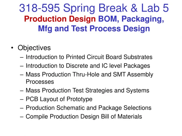
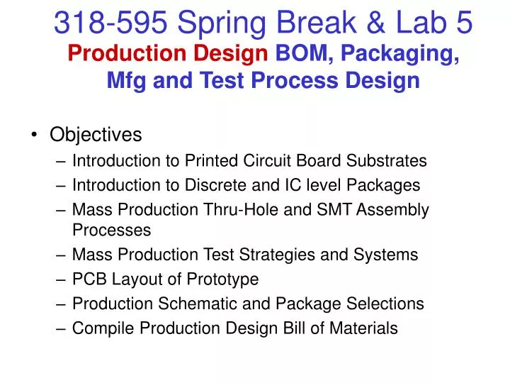
Production Design BOM, Packaging, Mfg and Test Process Design. Objectives Introduction to Printed Circuit Board Substrates Introduction to Discrete and IC level Packages Mass Production Thru-Hole and SMT Assembly Processes Mass Production Test Strategies and Systems PCB Layout of Prototype

E N D
Production Design BOM, Packaging, Mfg and Test Process Design • Objectives • Introduction to Printed Circuit Board Substrates • Introduction to Discrete and IC level Packages • Mass Production Thru-Hole and SMT Assembly Processes • Mass Production Test Strategies and Systems • PCB Layout of Prototype • Production Schematic and Package Selections • Compile Production Design Bill of Materials
Production Design BOM, Packaging, Mfg and Test Process Design • Recall Lab 3 - Prototyping
Prototype PCB Design - PreLAB • Deliverable Set 1: Individual Block Level - PROTOTYPE • PROTOTYPE Block BOM incl Packages • PROTOTYPE Schematic (Suggest Using ExpressSCH) • PROTOTYPE Netlist Table • PROTOTYPE EXPRESS-PCB Layout: Remember to Consider • Overall Dimensions & Sharing with Other Blocks • 2 Layers or 4 Layers • Component Package Matching your BOM and your Part Procurement • Through Hole Parts Preferred in Prototypes • Power & Ground Trace Widths, Signal Trace Widths • Silkscreen Labeling • Input & Output signal pads for wires/connectors and other off board signals
Production Design BOM, Packaging, Mfg and Test Process Design - PreLAB Production Design !! Not for Prototype Deliverable Set 2: Individual Block Level • Revise Your Detailed Block Production Schematic (from Lab 4) • For each design block, compile Block BOM template info • Using Excel Template, for each unique component define; • Qty • Primary Unit* • Tol%* • PCB Attach Method • # of Pins or Connections • Package Type • Placement Method • Mfg Part # for at least 2 sources if possible • Estimated PCB Area in mm2 • Unit Cost and Total Cost • Paste as picture only into PPT slide as part of block design or Summarize
Production Design BOM, Packaging, Mfg and Test Process Design For Production Assembly Only Not for Prototype • Create a Master Product Asm BOM for the Project by combining all Block BOMs • Eliminate redundant Part lines by combining Qty • Try to eliminate any similar components by choosing the same part when applicable • Use as few unique part numbers as possible in the overall design • Copy and Paste as picture only into PPT slide(s) as part of overall design • Create overall Mfg Process Diagram • Show all blocks related to PCB assembly • Show all blocks related to test • Include all levels of assembly Deliverable Set 3: Product Level - Team Remainder of Lab Time for Prototype Construction & Test
Production Design BOM, Packaging, Mfg and Test Process Design Production Design Guide • Use Mass Production Quantities Based on Business Case • Use Surface Mount Technology Whenever Possible • Costs to Consider • Parts and Material including Substrates (Fabs) • Assembly at All Levels • Test & Inspection • Programming, Setting & Configurations • ESS • Define # of Assembly levels (PCB, Cables, Display, Overall, etc) • Define Assembly process flow diagram(s) for each level • Optional Deliverables (Paper Only) • Assembly Level Diagram (Mechanical) • PCB Layouts