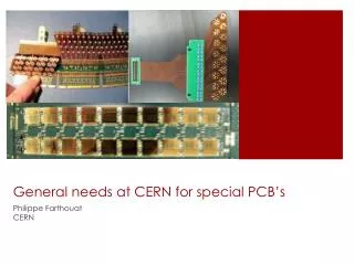
GEM を用いた MPGD
GEM を用いた MPGD. 2005 年 10 月 14 日 内田智久 KEK 測定器開発室. 村上武、仲吉一男、関本美智子、田中真伸、 池野正弘、氏家宣彦、宇野彰二( KEK) 中野英一(大阪市大) 杉山晃(佐賀大). Outline. GEM 応用 今後の予定. GEM foil. φ = 70μm. 10cm. 140 μm. 10cm. Scienergy Co., Ltd. 製. 5 μm. Polyimide. Cu. 50 μm. 5 μm. GEM detector. 55 Fe (5.9 keV X-ray). HV.

GEM を用いた MPGD
E N D
Presentation Transcript
GEMを用いたMPGD 2005年10月14日 内田智久 KEK 測定器開発室 村上武、仲吉一男、関本美智子、田中真伸、 池野正弘、氏家宣彦、宇野彰二(KEK) 中野英一(大阪市大) 杉山晃(佐賀大)
Outline • GEM • 応用 • 今後の予定
GEM foil φ = 70μm 10cm 140 μm 10cm Scienergy Co., Ltd. 製 5 μm Polyimide Cu 50 μm 5 μm
GEM detector 55Fe (5.9 keV X-ray) HV Drift plane HV Drift R GEM1 R Transfer-1 R GEM2 Transfer-2 R GEM3 Induction R R Readout pads Triple GEM detector
Test chamber Drift plane HV Gas GEM Pre-amp.
Pulse shape and spectrum 55Fe (5.9 keV X-ray) GEM foilからの信号 ED=0.5kV/cm ΔVGEM=325V ET=1.6kV/cm EI=3.3kV/cm 240mV Readout padからの信号 20ns Sigma/Mean≒8.8%
GEM Foil PCB
Gain (ΔVGEM) 104 ED=0.5kV/cm ET~1.6kV/cm EI ~ 3.2kV/cm ArCO2 (70:30) ED~0.5kV/cm ET~1.8kV/cm EI~3.6kV/cm P10 103 102
応用 X線吸収画像 TPC 中性子構造解析
GEMの利点 • 安価、大型化容易 • ガス検出器の特徴を生かす。 • ガス増幅部と読み出し部とが独立 • 多段化可能 • 低電場 放電を避けられる。 • 他の補助にも出来る • 高電場が局在 • 放電の抑制効果
TPC GEMを用いる利点 イオンフィードバックが少ない 非連続なワイヤー部分での ExB問題が避けられる 今後、信号のGEM部での拡がりの理解 佐賀大との協同
MPGD回路図解説 TM2005/6/17 4層(500μ)400mmSQ. FLAT40;CN8~1640P VATAx16chips GEM Spacer hole 3.2Φx4(117x117) PAD;ICPAD1~16(data ,cont 83pad) PAD;XVPAD1(data 250pad) PAD;YVPAD1(data 250pad) 補強板 PAD;YVPAD2(data 250pad) FLAT10;TWIST110P FLAT40;CN1~740P ストリップピッチ;400μ ストリップ幅 表面;20-100μ 裏面;340μ カプトン厚 50μ PAD;XVPAD2(data 250pad) 2層 (50μ) 110mmSQ. FLAT40;70mmx9mm :(80mmSQ.)x2個所 FLAT10;TWIST10P TM2005/8/9 オンラインエレキにて ;Bonding wire;(83x16+32x16+250x4=2840wires
今後の予定 • GEMの理解 • 信号の広がりなど • 2次元読み出し • 進行中 • 硬X線検出器 • 金メッキGEM • 中性子検出器 • ボロン蒸着GEM