Download
1 / 32
330 likes | 503 Views
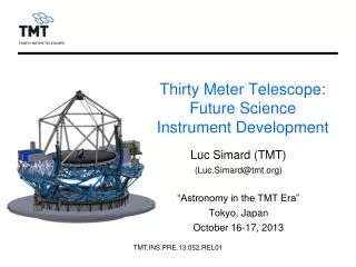
A Zero Noise Detector for the Thirty Meter Telescope. Status Update October 2012 Don Figer Director, CfD Professor, College of Science, RIT. Summary. We have produced a working 256x256 optical imager that detects single photons. dark current is low cross-talk is higher than we would like

E N D
A Zero Noise Detector for the Thirty Meter Telescope Status Update October 2012 Don Figer Director, CfD Professor, College of Science, RIT
Summary • We have produced a working 256x256 optical imager that detects single photons. • dark current is low • cross-talk is higher than we would like • quantum efficiency is ~20%, but can be increased • We are testing a 32x32 infrared imager that detects single photons • In the following year, we will fabricate an all-new design for the optical imager to reduce cross-talk and increase manufacturability.
First Light Image First Light Image with 256x256 Single Photon Detector
256x256 Readout IC 256×256 CMOS ROIC. This integrated circuit provides the control electronics for the detector. The light-sensitive area corresponds to the grey square near the center of the device.
Pixel Architecture (left) Cross section view of two neighboring low-fill-factor GM-APD structures showing the avalanche and absorber regions. Photons enter the GM-APD via backside illumination and are absorbed in the “absorber” regions. Charge is multiplied in the “multiplier” regions. (right) Cross section view of two neighboring high-fill-factor GM-APDs in which photoelectrons generated between pixels will diffuse and drift until they reach an absorber depletion region. The high-fill-factor architecture provides greater capability for the device to count every photon as an event.
pn Junction Geometries Experiment results showing dark count rate versus time delay from GM-APD rearm to subsequent firing (quench time) as measured by the inverse of the mean time to first detection event.The blue curve is for the LFF GM-APD with the truncated stepped boron implant, and the red curve is for the HFF GM-APD. The bottom architecture is superior for suppressing dark count.
Bump Bonding The left Image is an optical photograph of the indium bump formations on test structures and the right image is a scanning electron micrograph picture of indium bumps on the GM-APDs. The bumps, one per pixel, electrically connect the readout circuit to the light-sensitive diode array.
External Circuitry The left graphic shows the system diagram of the test electronics for the phase one detector. The right picture shows a custom electronics board fabricated to test the detector.
Raft Assembly (left) Image of detector mount, as seen through the side port of the dewar. There are four positions for detectors. The upper left position is occupied by a mechanical dummy unit. The other three positions are empty. (right) Mechanical raft assembly. The upper two positions are occupied by mechanical dummy units.
System Diagram System diagram of the cold electronics. The diagram only shows two cables from the detectors to the fanout board. In operation, there will be four cables, one for each detector.
Dark Current Dark Count Rate for a high fill-factor GM-APD device measured at varying cryogenic temperatures.
Imaging Analysis Image of a watch taken with a GM-APD device in a cryogenic camera system. The image was taken with the device cooled in the test system and a Nikon lens mounted on the optical window. The image is formed by the summation of single photon detections
Single photon detection Given a constant source, , if APD is sensitive to single photons, the trigger probability should evolve as P = 1 - exp(-Tgate) If 2 photons are required to trigger the APD, then P = 1 - exp(-Tgate) - Tgate exp(-Tgate) Real Data Tgate=
Crosstalk & Afterpulse P (Neighboring Pixel Triggered | Reference Pixel Triggered) 31 by 31 pixel region Afterpulse Crosstalk There is no strong evidence of afterpulsing
Personnel RIT personnel working on the Moore project (top to bottom, left to right): Tom Montagliano, Brandon Hanold, Don Stauffer, Brian Ashe, Donald Figer, Tom Praderio, Chris Maloney, John Frye, Max Bobrov.
Gordon MooreProgress and Plans Brian Aull 25 September 2012
Accomplishments Recent Dark count data collected from 256x256 passive imager, and successfully fit to simple analytic model Results show that crosstalk dominates dark count rate, native thermal dark count rate is low Defined the major elements of new trenching and hybridization processes and have begun development Long Term Remarkable progress in understanding APD design and performance issues, fabrication and process integration
Passive Imaging Demonstration • Back illuminated 256×256 APD arrays • High-fill-factor with deep implant step • 25-mm pixel pitch • Hybridized to PCROIC readout chip • Packaged and incorporated into camera for field demo • Successfully deployed to collect imagery • Dark count data from these devices collected and analyzed
Modeling Crosstalk • Dots are experimental data; solid curves show prediction of simple rate equation model • h is number of photoelectrons created by APD light emission, e is probability that such a photoelectron will trigger an APD that has not yet fired APD BIAS T=-30C -30.0V Probablity that a pixel has fired -29.5V -29.0V Time after ARM (ms)
Amorphous Silicon for Crosstalk Suppression aSi T, R Si • High attenuation, low reflection at wavelengths where crosstalk is worst • Good match to silicon thermal expansion coefficient • Process-compatible • Process development runs in progress l (nm)
Planned Work • Implement a hybridization technique based on Ziptronix Direct Bond Interconnect (DBI) process (funded by other sponsor) • Fabricate a lot of APDs on silicon-on-insulator (SOI) wafer and characterize (no CMOS readout) • SOI facilitates APD thickness customization and uniform back illumination • Fabricate and test 256×256 focal planes based on DBI hybridization of SOI APDs to the PCROIC readout chip (funded by other sponsor) • With further funding, do advanced trench process development/characterization and investigation of spectral quantum yield of light emission by Geiger-mode APDs DBI interconnects
Gordon MooreInGaAs APDsProgress and Plans Michael Grzesik 01 October 2012
CCS-0889-A 10 nm n+ -InGaAs contact Si>2e18 1 μm Si>2e18 n+ -InP cap 1.5 μm n<5e15 n-InP absorber 53.5 nm InP field stop Si:3.3e17 3 μm nid n-InP avalanche 1 μm Zn:8e17 p+ InP p+ InP 2 μm Zn:2e18 InP Substrate Previous Work • Initial measurements were aimed at measuring the Dark Count Rate (DCR) for InGaAs devices • Interarrival plots indicated afterpulsing • A circuit allowing for long holdoff times was designed for new measurements • DCR was determined using the tail end of the newly measured interarrival plots Hold-off 600 ms A1*e-λ1t + A2*e-λ2t λ1=51.3 Hz λ2=8.02 Hz
Previous Work 77 K Data 600 ms Hold-off • Measured DCR was much larger than expected • Afterpulsing is believed to still be present and dominating interarrival time data • Proposed work for 2012 included measuring the DCR using devices bonded to Read Out Circuits • The Read Out Circuits will reduce charge flowing through a device during breakdown mitigating afterpulsing. Data is ~ 2 orders of magnitude off from calculations
Present Modeling of Breakdown Voltage • Earlier breakdown voltage measurements show a discrepancy between measured and calculated values at cryogenic temperatures of ~5 V • A low temperature model for the electron and hole impact ionization coefficients has been constructed • The phonon mean free path and phonon energy were adjusted in the models to match low temperature data and predict breakdown • The new impact ionization coefficients allow for an accurate prediction of breakdown voltage allowing for accurate device growth and design
Planned Work Over Next 3 Months • Over the past year, hardware and software issues have hindered DCR measurements for APDs bonded to readout circuits. • It is believed the final software issue has been identified in the test setup and the setup will be functional in the next month. • DCR data will be taken and analyzed and compared with both the theoretical calculations and previous long holdoff time measurements. • Modeling work is focused on modifying the presently used impact ionization coefficient values so that the are valid in the 77K – 300K temperature range.
A New Funding Model… • GNSSTI seeks to disrupt the current paradigm of space science and exploration to drive scientific discovery at an accelerated pace, and address questions that inspire us all • Scientific exploration of space holds promise to address some of humankind’s most compelling questions: Where did we come from? What is the nature and fate of the Universe? Are we alone? • Answering these questions is mired in small, single-investigator-focused funding models and large, expensive, government-managed space missions using old technology. • Answers are within our reach, if we use new approaches that leverage truly interdisciplinary, international teams, emerging technologies, and new spaceflight approaches.
Why now? • NASA budget constraints will limit space science program content during the next decade • Federal discretionary spending will be capped • Significant emphasis on applied research across Federal science • Large ground-based telescopes with significant private funding now cost as much as capable space missions • We have the opportunity seize this moment in time by bringing the creativity of the “New Space” community to space science and exploration. • For example, there’s a window this decade when NASA will not launch any mission capable of exoplanet imaging or that returns samples from Mars • NASA Astrophysics will not start any new large mission until after JWST launches (NET 2018), likely to be followed by WFIRST wide-field infrared telescope • NASA Planetary Science likely facing a near-term budget decrease and is expected to consider alternatives to a sample return mission/strategy for remaining Mars launches before 2020
Plan • Permanently establish and maintain a world-class worldwide research organization with the resources, personnel, and facilities to drive rapid progress in our understanding of the Universe and life within it • In the next decade, create and execute first-of-a-kind, opportunistic projects to advance fundamental scientific knowledge of our Universe and the life within it
Citizen Science & Outreach • Disseminate frontier scientific discoveries to the public through existing and experimental media, including involving citizens in design and data analysis opportunities where appropriate • Inspire and train the next generation of scientists and engineers in team-based, interdisciplinary, world-class research • Create U.S. network of University, Institute and other non-profit scientific partners • Create a structurally entrepreneurial global network to explore the Universe • International interest is high, and possibly enabling
Principles • Commitment to creative excellence • Commitment to scientific truth • Flexible Perseverance • Openness and transparency
![[79.03] The Thirty Meter Telescope (TMT) Project](https://cdn1.slideserve.com/1737456/79-03-the-thirty-meter-telescope-tmt-project-dt.jpg)