Download

1 / 2
0 likes | 10 Views
Semiconductor Industry Growth: The ongoing growth of the semiconductor industry, fueled by increasing demand for electronic devices, is driving the need for advanced wafer processing equipment.<br>Technological Advancements: Continuous advancements in semiconductor technology, such as the development of smaller and more powerful devices, require sophisticated wafer deposition techniques.<br>

E N D
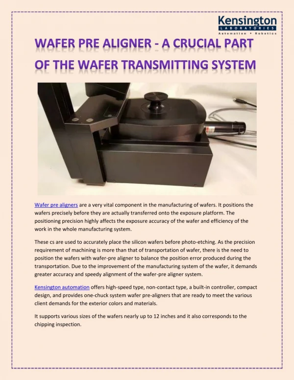
+1 217 636 3356 +44 20 3289 9440 sales@mobilityforesights.com Your Cart 0 Company Market Reports Consumer Research Advisory Services Exports - Imports Careers Contact Us Blog Your cart is empty Your Name Return to Shop Business Email Global Wafer Plasma Deposition System Market 2023-2030 Country Phone Number +82 Company Name Single User License : $ 4,000 Your message Corporate User License : $ 6,000 By submitting this form, you are agreeing to the Request Sample Terms of Use and Privacy Policy. I'm not a robot reCAPTCHA Privacy - Terms BUY NOW DOWNLOAD SAMPLE DESCRIPTION TABLE OF CONTENTS GLOBAL WAFER PLASMA DEPOSITION SYSTEM MARKET INTRODUCTION Chemical vapour deposition techniques like Wafer Plasma Deposition System are used to produce thin coatings on a substrate that transition from a gaseous to a solid state. Following the formation of a plasma of the interacting gases, chemical reactions are involved in the process. Radio frequency (RF), alternating current (AC), or direct current (DC) discharge between two electrodes, the space between which is filled with the reacting gases, is typically how the plasma is produced. A huge perforated metal plate that is situated above the sample acts as a shower head, allowing reactant (and dilution) gases to enter the process chamber. The shower head aids in distributing reactant gas flow over the sample surface more uniformly. To create a plasma, an RF potential is given to the shower head. In order to produce more chemically reactive radicals, energetic electrons in the plasma ionise or dissociate (or “crack”) reactant gases. To create the thin layer of deposition material covering the sample, these radicals react. The main benefit of lower process temperatures for Wafer Plasma Deposition System over LPCVD, where all of the energy for reaction is thermally supplied, is energy supplied by plasma. GLOBAL WAFER PLASMA DEPOSITION SYSTEM MARKET SIZE AND FORECAST We use cookies to understand site usage and improve content and offerings on our site. To learn more, refer to our Privacy Policy. By continuing to use this site, or closing this box, 0 Learn more you consent to our use of cookies. Got it! Send message Continue Shopping The Global Wafer Plasma Deposition System market accounted for $XX Billion in 2022 and is anticipated to reach $XX Billion by 2030, registering a CAGR of XX% from 2023 to 2030. MARKET DYNAMICS CVD, or Chemical Vapour Deposition HDP-CVD, or Wafer Plasma Deposition System enhanced by plasma dependable systemsDevices for Advanced Memory, Analog and Mixed Signal, Discrete and Power, Interconnect, packaging, patterning, sensors & transducers, optoelectronics & photonics, TransistorDeposition methods, which are widely used in the chip manufacturing process, deposit a variety of insulating and conducting materials on the wafer to assist create the structural elements and wiring of a semiconductor device. Due to the variety of feature forms and materials, non-traditional chip industries including micro-electromechanical systems (MEMS) and power devices have more complex production needs. The production-tested deposition solutions in Lam’s Reliant product family offer the process flexibility, dependable performance at high productivity, and low cost of ownership (CoO) required for these applications. COMPANY PROFILE Lam Research Corporation ASM International N.V Veeco Instruments Inc. CVD Equipment Corporation Aixtron SE Buhler Alzenau THIS REPORT WILL ANSWER FOLLOWING QUESTIONS 1. How many Wafer Plasma Deposition Systems are manufactured per annum globally? Who are the sub-component suppliers in different regions? 2. Cost breakup of a Global Wafer Plasma Deposition System and key vendor selection criteria 3. Where is the Wafer Plasma Deposition System manufactured? What is the average margin per unit? 4. Market share of Global Wafer Plasma Deposition System market manufacturers and their upcoming products 5. Cost advantage for OEMs who manufacture Global Wafer Plasma Deposition System in-house 6. key predictions for next 5 years in Global Wafer Plasma Deposition System market 7. Average B-2-B Wafer Plasma Deposition System market price in all segments 8. Latest trends in Wafer Plasma Deposition System market, by every market segment 9. The market size (both volume and value) of the Wafer Plasma Deposition System market in 2023-2030 and every year in between? 10. Production breakup of Wafer Plasma Deposition System market, by suppliers and their OEM relationship RELATED REPORTS MARKET REPORTS CONSUMER INFORMATION ADVISORY CONTACT INFORMATION
RESEARCH SERVICES 172/1, 2nd Floor, 5th Main, 9th Cross Rd, Opposite to Kairalee Nikethan Education Trust, Indira Nagar 1st Stage, Bengaluru, Karnataka 560038, INDIA +1 217 636 3356, +44 20 3289 9440 sales@mobilityforesights.com Working Hours: Mon - Fri (9 AM - 9 PM IST) Connect with us © Copyright 2017-2023. Mobility Foresights. All Rights Reserved.