Download
1 / 7
70 likes | 87 Views
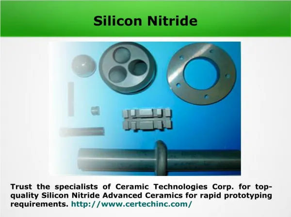
Stoichiometric silicon nitride is used as an insulator while low-stress nitride is used for making membranes which are resistant to HF etching.<br>https://waferpro.com/silicon-wafers/silicon-nitride-wafers/

E N D
The applications and uses of LPCVD silicon nitride deposition method for manufacturing silicon wafers
Thin films are deposited onto substrates for use as functional components of a device, like for creating an insulation or conduction layer. The layer can be applied for the etching process where it is usually removed after the process is over. Thin films of silicon nitride are used as these display dielectric properties. Silicon nitride is a dielectric material used in the processing of semiconductors. The material can be used on a wide variety of substrates using LCPCVD (Low Pressure Chemical Vapor Deposition) and other techniques such as sputtering and evaporation. The process can be completed in a hot-wall or cold-walled quartz tube reactor. Hot-walled furnaces have high throughput and thermal uniformity, resulting in uniform films. However, deposition can occur on walls in hot furnaces, requiring more maintenance for cleaning. Cold wall reactors have lower maintenance as no film deposition occurs on the reactor walls.
In the process of LPCVD silicon nitride deposition, the tube is evacuated to low pressures. Once the tube is under vacuum, it is then heated up to deposition temperature at which the precursor gas decomposes. The gas is injected into the tube where it diffuses and reacts with the surface of the substrate, resulting in a solid material. Any excess gas is pumped out of the tube through an abatement system. LPCVD films are typically more uniform and lower in defects.
Use of polysilicon Silicon is deposited using the LPCVD silicon nitride deposition method on the silicon wafers. Most LPCVD films are somewhat conformal and can offer protection for structures requiring electrical isolation. Polysilicon can be deposited on both doped and P- and N-doped silicon wafers. Polysilicon is used as wire traces for integrated circuits and MEM devices. Silicon nitride can be deposited in both stoichiometric form and low-stress form through the process of LPCVD silicon nitride deposition, depending upon the required material properties. Stoichiometric silicon nitride is used as an insulator while low-stress nitride is used for making membranes which are resistant to HF etching.
Silicon wafers with various types of depositions At WaferPro, you can get the best quality silicon wafers for use in specific applications. The company uses LPCVD silicon nitride deposition method using state-of-the-art technology so that what you get is of the highest standards. WaferPro offers silicon wafers with stoichiometric LPCVD silicon nitride deposition or low-stress LPCVD nitride, as well as super low-stress LPCVD nitride. The company also offers high-quality PECVD nitride, low-stress PECVD nitride, and PECVD OxyNitride. Wafer diameters are available from 2” to 12” (300 mm), and nitride thickness is available from 100Å to 20,000Å.
WaferProis the leading supplier of silicon wafers and semiconductor materials to the electronics industry and research institutes. The company offers Prime and Test silicon wafers that adhere to SEMI standards in a variety of diameters. In addition to SEMI standard silicon wafers, WaferPro also offers Float Zone (FZ) wafers, Silicon on Insulator (SOI) wafers, and other semiconductor materials. Double-side polished, oxide MEMS wafers are also available.
CONTACT INFORMATION https://waferpro.com/ sales@waferpro.com (408) 622-9129 https://waferpro.com/silicon-wafers/silicon-nitride- wafers/