Download
1 / 5
50 likes | 61 Views
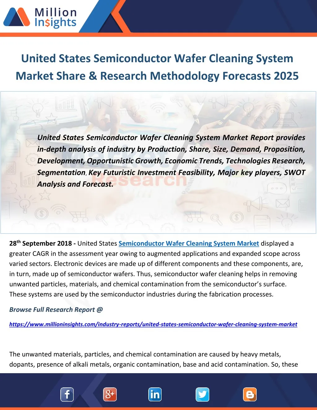
United States semiconductor wafer cleaning system market displayed a greater CAGR in the assessment year owing to augmented applications and expanded scope across varied sectors. Electronic devices are made up of different components and these components, are, in turn, made up of semiconductor wafers. Thus, semiconductor wafer cleaning helps in removing unwanted particles, materials, and chemical contamination from the semiconductor’s surface. These systems are used by the semiconductor industries during the fabrication processes.<br>

E N D
United States Semiconductor Wafer Cleaning System Market Share & Research Methodology Forecasts 2025 United States Semiconductor Wafer Cleaning System Market Report provides in-depth analysis of industry by Production, Share, Size, Demand, Proposition, Development, Opportunistic Growth, Economic Trends, Technologies Research, Segmentation, Key Futuristic Investment Feasibility, Major key players, SWOT Analysis and Forecast. 28th September 2018 - United States Semiconductor Wafer Cleaning System Market displayed a greater CAGR in the assessment year owing to augmented applications and expanded scope across varied sectors. Electronic devices are made up of different components and these components, are, in turn, made up of semiconductor wafers. Thus, semiconductor wafer cleaning helps in removing unwanted particles, materials, and chemical contamination from the semiconductor’s surface. These systems are used by the semiconductor industries during the fabrication processes. Browse Full Research Report @ https://www.millioninsights.com/industry-reports/united-states-semiconductor-wafer-cleaning-system-market The unwanted materials, particles, and chemical contamination are caused by heavy metals, dopants, presence of alkali metals, organic contamination, base and acid contamination. So, these
impurities are removed with the help of semiconductor wafer cleaning systems. In wafer cleaning process, various steps are involved such as particulate removal clean, pre diffusion clean, film removal, metallic ion removal, and post etch clean. The factors that are responsible for driving the market growth include rising demand for single wafer processing, increasing demand for printed electronics, growing consumer electronics and semiconductor industries. The other factors include miniaturization of electronic devices, increasing demand of portable consumer electronics devices, reducing thickness of circuit systems, and improving quality standards of production. However, stern & changing quality standards and lack of skilled workforce may negatively impact the semiconductor wafer cleaning system market growth. The market is categorized based on technology, equipment, applications, and geography. United States semiconductor wafer cleaning system market is classified by technology as vapor cleaning technology, cryogen aerosol based cleaning technology, fine particle detection technology, local area cleaning technology, and supercritical fluid based cleaning technology. United States semiconductor wafer cleaning system market is classified by equipment as semi-automated wet batch system, rotary wafer etching system, scrubbers, and manual wet batch system. Request Sample Copy of this Market Research @ https://www.millioninsights.com/industry-reports/united-states-semiconductor-wafer-cleaning-system-market/request-sample United States semiconductor wafer cleaning system market is segmented by application as chemical contamination, metallic contamination, and particle contamination. United States semiconductor wafer cleaning system market is segregated by geography as Southwest, The West, New England, The Middle Atlantic, The South, and The Midwest. United States is expected to be the largest market for semiconductor wafer cleaning systems due to increasing electronics industries and semiconductor production. The key players contributing to the robust development of the United States semiconductor wafer cleaning system industry may include Planar Semiconductor, Tokyo Electron, Dainippon Screen, Akrion, Lam Research, Modutek, MEI Wet, Cleaning technologies, SEMES and Falcon. The manufactures are emphasizing on the inorganic growth to keep pace with the cutthroat competition
in the market. Consequently, mergers, acquisitions, and joint ventures have come up as important strategies. Market Segment: Geographically, this report splits the United States market into seven regions: • The West • Southwest • The Middle Atlantic • New England • The South • The Midwest with sales (volume), revenue (value), market share and growth rate of Semiconductor Wafer Cleaning System in these regions, from 2013 to 2025 (forecast). See More Reports of this Category by Million Insights @ https://www.millioninsights.com/industry/semiconductor United States Semiconductor Wafer Cleaning System market competition by top manufacturers/players, with Semiconductor Wafer Cleaning System sales volume, price, revenue (Million USD) and market share for each manufacturer/player; the top players including • Dainippon Screen • Tokyo Electron • Lam Research • Akrion • MEI Wet
• Modutek • SEMES • Cleaning technologies • Falcon • Planar Semiconductor On the basis of product, this report displays the production, revenue, price, market share and growth rate of each type, primarily split into • Rotary Wafer Etching System • Wet Batch System • Others On the basis on the end users/applications, this report focuses on the status and outlook for major applications/end users, sales volume, market share and growth rate for each application, including • Particle Contamination • Metallic Contamination • Chemical Contamination • Others Browse Full Research Report @ https://www.millioninsights.com/industry-reports/united-states-semiconductor-wafer-cleaning-system-market
Get in touch At Million Insights, we work with the aim to reach the highest levels of customer satisfaction. Our representatives strive to understand diverse client requirements and cater to the same with the most innovative and functional solutions. Contact Person: Ryan Manuel Research Support Specialist, USA Email: ryan@millioninsights.com Global Headquarters Asia Pacific Million Insights Million Insights Felton Office Plaza 6265 Highway 9 Felton, California 95018, United States Office No. 302, 3rd Floor, Manikchand Galleria, Model Colony, Shivaji Nagar, Pune, MH, 411016 India Phone: 1-408-610-2300 Email: sales@millioninsights.com Phone: 91-20-65300184 Email: sales@millioninsights.com Visit Our Blog: www.millioninsights.blogspot.com