Download
1 / 4
0 likes | 13 Views
Take your career to the next level with Takshila-vlsi.com online physical design training. Improve your abilities and acquire practical experience from the convenience of your own home.

E N D
Online Physical Design Training | Takshila-vlsi.com Take your career to the next level with Takshila-vlsi.com online physical design training. Improve your abilities and acquire practical experience from the convenience of your own home. online physical design training
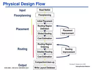
About Us: - Analog Layout Design / Custom Layout Design / IC design training course mainly focused on giving hands-on practical exposure in doing chip layout design for a given analog & mixed signal design. By end of the course you will learn to work in Linux environment, schematic entry in EDA tool, placement planning, analog and digital layout design, routing and physical verification checks like DRC, LVS for typical analog circuits such as Opamp, PLL, Bandgap, LDO and standard cells. You will also understand fixing deep sub-micron process issues like Antenna, Latchup, EM&IR. Course also focus on giving insights of the Analog circuit design and Simulation, IO Layout Training, Memory Layout Training as well. After completing the course, you will get opportunity to move into domains such as Analog & Mixed Signal Layout Design, Memory Layout Design, Standard Cell Layout Design, and I/O Layout Design.
Takshila Institute of VLSI Technologies 39/4, 2nd Floor, Kishan Arcade, erns City Road Mahadevapura,Bengaluru Karnataka 560048 India Contact us:-