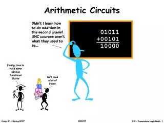

Arithmetic Circuits
E N D
Presentation Transcript
Arithmetic Circuits Dr. ShrutiJamsandekar Assistant Professor CSIBER, Kolhapur
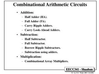
Topics covered • Combinational circuits • Addition circuits • Multiplication circuits • Clocked circuits
Combinational Circuits Depth of a circuit corresponds to its "running time." full adder : building block of most of the combinational circuit.
Combinational Circuits • Combinational circuits operate in parallel: • many elements can compute values simultaneously as a single step. • Combinational elements • Arithmetic circuits in real computers are built from combinational elements that are interconnected by wires. • A combinational element is any circuit element that has a constant number of inputs and outputs and that performs a well-defined function. • Boolean combinational elements-- inputs and outputs are all drawn from the set {0,1}, where 0 represents FALSE and 1 represents TRUE.
Combinational elements A boolean combinational element that computes a simple boolean function is called a logic gate. Figure below shows the four basic logic gates that will serve as combinational elements : The operation of each gate, and of any boolean combinational element, described by a truth table
Combinational elements • We use the symbols to denote functions • ┐NOT function • ˄ AND function • ˅ OR function • XOR function Thus, for example, 0 1 = 1. • propagation delay of the element - time differential between input values settle, or become stable on entering a combinational element and the element's output value to become both stable and correct.
Combinational circuits A combinational circuit consists of one or more combinational elements interconnected in an acyclic fashion. • The interconnections are called wires. • A wire can connect the output of one element to the input of another. • The number of element inputs fed by a wire is called the fan-out of the wire. • If no element output is connected to a wire, the wire is a circuit input, accepting input values from an external source. • If no element input is connected to a wire, the wire is a circuit output, providing the results of the circuit's computation to the outside world. • Combinational circuits contain no cycles and have no memory elements.
Full adders Figure below shows a combinational circuit, called a full adder, that takes as input three bits x, y, and z. It outputs two bits, s and c, according to the following truth table: Outputs is the parity of the input bits, s = parity(x,y,z) = x y z, Outputc is the majority of the input bits, c= majority(x,y,z) = (xy) (yz) (xz).
Full Adder operation A full-adder circuit. (a) At time 0, the input bits shown appear on the three input wires. (b) At time 1, the values shown appear on the outputs of gates A-D, which are at depth 1. (c) At time 2, the values shown appear on the outputs of gates E and F, at depth 2. (d) At time 3, gate G produces its output, which is also the circuit output.
Circuit depth &size • Measure the propagation delay of a combinational circuit in terms of the largest number of combinational elements on any path from the inputs to the outputs. • Thedepth of a circuit, corresponds to its worst-case "running time," inductively in terms of the depths of its constituent wires. The depth of an input wire is 0. • If a combinational element has inputs x1, x2, . . . ,xn at depths d1, d2, . . . ,dn respectively, then its outputs have depth max{d1, d2, . . . ,dn} + 1. • The depth of a combinational element is the depth of its outputs. • The depth of a combinational circuit is the maximum depth of any combinational element. • The sizeof a combinational circuit is the number of combinational elements it contains.
Addition Circuit • Combinational circuit to perform addition of 2 n bits binary numbers • Ripple carry addition -- O(n) • Carry lookahead adder – O(log n) • Carry save addition– O(1)
Addition circuits Adding numbers represented in binary. We start with the ordinary method of summing binary numbers. We assume that a nonnegative integer a is represented in binary by a sequence of n bits an-1, an-2, . . . , a0, where nlg(a + 1) and Given two n-bit numbers a = an-1, an-2, . . . , a0 and b = bn-1, bn-2, . . . , b0, we wish to produce an (n + 1)-bit sum s = sn, sn-1, . . . , s0. Adding two 8-bit numbers a = 01011110 and b = 11010101 to produce a 9-bit sum s = 100110011. Each bit ci is a carry bit. Each column of bits represents, from top to bottom, ci, ai, bi, and si for some i. Carry-in c0 is always 0.
Ripple-carry addition Ann-bit ripple-carry adder is formed by cascading n full adders FA0, FA1, . . . , FAn-1, feeding the carry-out ci+1 of FAi directly into the carry-in input of FAi+1. Figure shows an 8-bit ripple-carry adder. The carry bits "ripple" from right to left. The carry-in c0 to full adder FA1 is hardwired to 0, that is, it is 0 no matter what values the other inputs take on. The output is the (n+1)-bit number s = sn, sn-1, . . . , s0, where snequals cn, the carry-out bit from full adder FAn.