Download
1 / 4
0 likes | 14 Views
Pulraj Electronics Pvt. Ltd. focuses on providing high-quality printed circuit board manufacturing solutions. Understanding the circuit board manufacturing process is critical for producing dependable, high-performance devices. This blog will walk you through the critical phases needed, from the PCB layout approach to the final PCB design process, ensuring that you are knowledgeable and prepared to tackle your next project.

E N D
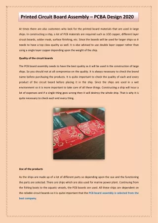
Pulraj Electronics Pvt. Ltd. focuses on providing high-quality printed circuit board manufacturing solutions. Understanding the circuit board manufacturing process is critical for producing dependable, high-performance devices. This blog will walk you through the critical phases needed, from the PCB layout approach to the final PCB design process, ensuring that you are knowledgeable and prepared to tackle your next project. Understanding the PCB Design Methods or Process The PCB design technique is the first and most critical step in circuit board manufacturing. Using superior format software programs like Altium Designer, KiCAD, or Eagle, engineers create a schematic diagram that outlines the electrical connections between components. This schematic is then translated into a bodily layout that optimizes factor placement, routing, and sign integrity. The PCB format should ensure that the board meets electric-powered, thermal, and mechanical necessities. Thorough simulations and testing are essential at this degree to prevent troubles like signal interference, strength loss, or warmth build-up. A nicely completed PCB assembly step is the key to reaching a practical and reliable final product.
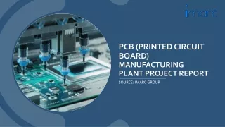
PCB Production Steps: Turning Design into Reality Once the design is finalized, the following section is PCB manufacturing. This consists of numerous critical steps that remodel the design into a useful circuit board. 1. Printing the Circuit Design The first step in PCB production is to transfer the layout onto the copper-clad board using photolithography. A light-touchy material is applied to the board, and the circuit layout is projected onto the material for the usage of ultraviolet (UV). This manner defines the conductive lines and pads needed to be a part of additives. 2. Etching the Copper Layer The next step is etching, wherein more copper is chemically removed, leaving the best copper traces that form the circuit’s pathways. This step ensures that the board will conduct energy wherever needed and insulate in which appropriate. 3. Drilling Holes Many PCBs require holes for thin leads or vias (connections among layers). These holes are drilled with precision to make sure the components will fit and the electrical connections can be set up properly. 4. Layering and Laminating For multi-layer PCBs, more than one layer of copper and insulating material are stacked and laminated collectively. The layers are aligned and heated to create a solid, multi-layer PCB able to handle more complex circuitry. 5. Testing the PCB Before moving directly to assembly, the PCB is carefully tested. Electrical checks are executed to check for defects which include short circuits or open circuits. This is essential to make sure that the electronics manufacturing process has been completed successfully and the board functions as meant.
The PCB Assembly Steps After the PCB is produced, it enters the PCB design process, wherein additives are set up on the board. 1. Solder Paste Application The first step in PCB assembly includes making use of solder paste on the board’s pads with the use of a stencil. The paste will later be melted to attach the components securely. 2. Placing the Components Automated choose-and-place machines are used to area components like resistors, capacitors, and ICs exactly onto the board. This step is vital for maintaining accuracy and consistency at some point in the meeting. 3. Soldering the Components Once the components are positioned, the board is handed through a reflow oven in which the solder paste melts, bonding the components to the board. This step guarantees that the additives are securely attached and electrically related. 4. Inspection and Testing After soldering, the PCB undergoes a thorough inspection to hit upon any defects. Automated Optical Inspection (AOI) or X-ray inspection can be used to ensure no component is lacking, misaligned, or improperly soldered. 5. Final Testing The final step in the PCB meeting is electric checking out. The board is powered immediately to ensure all additives are functioning well and that the PCB meets its layout specifications. This step verifies that the circuit board is ready for integration into the very last product. Conclusion At Pulraj Electronics Pvt. Ltd., we're devoted to supplying complete solutions for the printed circuit board manufacturing process. From the initial PCB design procedure to the very last PCB manufacturing steps and PCB design process, we make certain that each degree is dealt with with precision and understanding. Whether you’re working on a new product or need an
exceptional PCB meeting, we're here to be your dependent-on accomplice within the electronics manufacturing system. Reach out to us these days for all your PCB production desires!