Download
1 / 2
0 likes | 31 Views
The semiconductor industry is a critical sector in the global economy, with a wide range of applications across various industries. The use of hydrogen in the semiconductor industry has the potential to revolutionize the manufacturing process, leading to increased efficiency, reduced costs, and improved product quality.<br><br>

E N D
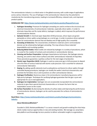
The semiconductor industry is a critical sector in the global economy, with a wide range of applications across various industries. The use of hydrogen in the semiconductor industry has the potential to revolutionize the manufacturing process, leading to increased efficiency, reduced costs, and improved product quality. DOWNLOAD PDF: https://www.marketsandmarkets.com/industry-practice/RequestForm.asp 1.Hydrogen Annealing: Processes for hydrogen annealing are used to enhance the structural and electrical characteristics of semiconductor materials, especially silicon wafers. In order to eliminate impurities and fix crystal defects, hydrogen is added, which improves the performance of semiconductor devices. 2.Epitaxial Growth: In chemical vapor deposition (CVD) processes, silicon layers are grown epitaxially on silicon wafers using hydrogen as a carrier gas. In order to produce silicon epitaxial layers for semiconductor devices that are flawless and of high quality, this is essential. 3.Annealing of Dielectrics: The characteristics of dielectric materials used in semiconductor devices can be enhanced by hydrogen annealing. This may enhance these materials' dependability and insulating qualities. 4.Reducing Metal Oxides: Metal oxides are reduced by hydrogen in a variety of procedures, which is crucial for the creation of contacts and connections in semiconductor devices. 5.Cleaning and Surface Preparation: Hydrogen-based plasma techniques, like hydrogen plasma cleaning, are used to clean silicon surfaces and other semiconductor materials of impurities. These procedures guarantee a spotless surface for the next stages of production. 6.Atomic Layer Deposition (ALD): Hydrogen is used as a precursor gas in ALD processes to deposit ultra-thin films of various materials with atomic-scale precision. ALD is essential for advanced semiconductor fabrication. 7.Doping: By adding specific elements (such as phosphorus and boron) to silicon wafers through controlled doping procedures, hydrogen can modify the wafers' electrical characteristics and promote the formation of p-n and d junctions on other semiconductor devices. 8.Hydrogen Purification: Numerous steps in the semiconductor manufacturing process call for high-purity hydrogen. Techniques for purifying hydrogen guarantee that the gas is pure and appropriate for use in vital applications. 9.Hydrogen Ion Implantation: Hydrogen ions are occasionally incorporated into semiconductor materials to give them special electrical characteristics or to lessen the harm that ion implantation causes to the crystal. 10.Surface Passivation: By decreasing the density of surface states and improving the performance of semiconductor devices, hydrogen can be used to passivate the surfaces of semiconductor materials. Read More: https://www.marketsandmarkets.com/industry-practice/hydrogen/semiconductors- industry About MarketsandMarkets™ Founded in 2010, MarketsandMarkets™ is a sector research and growth-enabling firm that helps clients realize revenue opportunities in new and existing markets. We leverage our proprietary data platform and Knowledge Services practice to deliver actionable insights to organizations.
The B2B economy is predicted to see the emergence of $25 trillion of new revenue streams that will displace existing workstreams. KnowledgeStore, our AI-driven market intelligence platform, serves as the discovery and validation engine to evangelize these new growth opportunities. In March 2023, Forbes recognized MarketsandMarkets as one of America’s Best Management Consulting Firms. To know more, visit:http://www.marketsandmarkets.com. Contact: Mr. Aashish Mehra MarketsandMarkets™ INC. 630 Dundee Road Suite 430 Northbrook, IL 60062 USA: 1-888-600-6441