Download
1 / 3
0 likes | 0 Views
The real power of SPM microscopy lies in its ability to bridge the gap between observation and manipulation. In materials science, where properties like surface roughness, adhesion, and conductivity dictate performance, having this level of insight is game-changing.

E N D
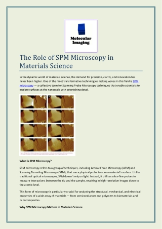
The Role of SPM Microscopy in Materials Science In the dynamic world of materials science, the demand for precision, clarity, and innovation has never been higher. One of the most transformative technologies making waves in this field is SPM microscopy — a collective term for Scanning Probe Microscopy techniques that enable scientists to explore surfaces at the nanoscale with astonishing detail. What is SPM Microscopy? SPM microscopy refers to a group of techniques, including Atomic Force Microscopy (AFM) and Scanning Tunneling Microscopy (STM), that use a physical probe to scan a material’s surface. Unlike traditional optical microscopes, SPM doesn’t rely on light. Instead, it utilizes ultra-fine probes to measure interactions between the tip and the sample, resulting in high-resolution images down to the atomic level. This form of microscopy is particularly crucial for analyzing the structural, mechanical, and electrical properties of a wide array of materials — from semiconductors and polymers to biomaterials and nanocomposites. Why SPM Microscopy Matters in Materials Science
The real power of SPM microscopy lies in its ability to bridge the gap between observation and manipulation. In materials science, where properties like surface roughness, adhesion, and conductivity dictate performance, having this level of insight is game-changing. For instance, in the development of next-generation electronics, SPM can identify inconsistencies at the atomic level that could affect conductivity. In biomaterials, it helps in understanding the topography and mechanical properties critical to biocompatibility. These insights enable researchers to fine-tune materials before they go into real-world applications. The Precision of Molecular Imaging As the capabilities of SPM microscopy expand, so does the importance of reliable tools and platforms. That’s where Molecular Imaging stands out. Known for its cutting-edge microscopy systems, Molecular Imaging has been at the forefront of helping materials scientists unlock the microscopic world with precision and ease. Their advanced instruments are engineered to deliver superior performance, whether you’re mapping the topography of a nanostructured surface or analyzing the electrical conductivity of thin films. With intuitive software and robust hardware, Molecular Imaging’s solutions empower researchers to achieve repeatable, high-resolution results across a wide spectrum of materials. Real-World Applications Nanotechnology — Designing nanoscale devices requires tools like SPM to evaluate and perfect fabrication processes. Energy Materials — From solar panels to batteries, understanding the surface properties of energy materials improves efficiency and longevity. Polymers and Composites — SPM helps in characterizing filler dispersion and surface modification effects, which are vital for product performance. Corrosion and Wear — By examining how materials degrade on the surface level, engineers can develop longer-lasting and more durable products. Looking Ahead As materials science pushes the boundaries of what’s possible, the role of SPM microscopy will only grow more central. Tools developed by innovators like Molecular Imaging are not just enabling discovery — they are shaping the future of materials engineering. Whether it’s unlocking the secrets of graphene or ensuring the structural integrity of medical implants, SPM microscopy is the lens through which we see — and shape — the materials of tomorrow. Contact us:
Email Id: songxu@nanocuetech.com Phone Number: 1-888-644-0389 Website: https://miafm.com/ Address: 3485 Middle belt, West Bloomfield, Michigan, 48323