Download

1 / 2
0 likes | 11 Views
The bright field water defect inspection system market is witnessing substantial growth due to the increasing emphasis on quality control and safety in water treatment processes. These inspection systems utilize bright field microscopy techniques to detect defects and contaminants in water sources, ensuring compliance with regulatory standards and enhancing the safety of drinking water.

E N D
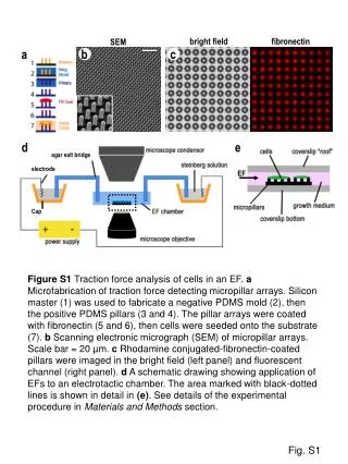
+1 217 636 3356 +44 20 3289 9440 sales@mobilityforesights.com Your Cart 0 Company Market Reports Consumer Research Advisory Services Exports - Imports Careers Contact Us Blog Your cart is empty Your Name Return to Shop Business Email Global Bright Field Wafer Defect Inspection System Market 2024- 2030 Country Phone Number +82 Company Name Single User License : $ 4,000 Your message Corporate User License : $ 6,000 . By submitting this form, you are agreeing to the Terms of Use and Privacy Policy. I'm not a robot Request Sample reCAPTCHA Privacy - Terms DOWNLOAD SAMPLE BUY NOW DESCRIPTION TABLE OF CONTENTS BRIGHT FIELD WAFER DEFECT INSPECTION SYSTEM MARKET INTRODUCTION TO BRIGHT FIELD WAFER DEFECT INSPECTION SYSTEM MARKET The factory’s mainstay technology, brightfield inspection, measures light coming from a higher angle. It illuminates a wafer using broadband light. The light is then captured, and a digital image is created. Brightfield measures light reflected between 25 to 30 degrees. It’s between 30 and 40 degrees in Greyfield. By identifying faults at an early stage and preventing yield losses, step-by-step scanning for defect inspection helps semiconductor producers. Expand every Bright-field microscopy advantages The colour of the visible structures is not altered by the optics. Certain structures are made visible by stains. Less setup is needed for bright-field microscopy in order to view the samples. finding errors or flaws in the programme where its performance is poor or does not meet its specifications; A test that causes the system to behave erroneously and hence reveals a flaw in the system is successful. BRIGHT FIELD WAFER DEFECT INSPECTION SYSTEM MARKET SIZE AND FORECAST We use cookies to understand site usage and improve content and offerings on our site. To learn more, refer to our Privacy Policy. By continuing to use this site, or closing this box, 0 Learn more you consent to our use of cookies. Got it! Send message Continue Shopping The Global Bright Field Wafer Defect Inspection System market accounted for $XX Billion in 2023 and is anticipated to reach $XX Billion by 2030, registering a CAGR of XX% from 2024 to 2030. BRIGHT FIELD WAFER DEFECT INSPECTION SYSTEM MARKET NEW PRODUCT LAUNCH The LS9600 is a new system from Hitachi High-Tech Company that can find particles and flaws on non-patterned bright field wafer deface inspection surfaces. When compared to our previous generation systems, it has a new high-output, short-wavelength laser that increases throughput at the sensitivity levels necessary for the mass production of cutting-edge semiconductor devices by about 2.6 times. With the launch of this product, Hitachi High-Tech will continue to support customers’ mass production of semiconductor devices by enhancing yields and lowering inspection expenses.Non-patterned wafer inspection systems are used for tasks including managing particles and flaws in semiconductor device manufacturing machinery and monitoring the state of non- patterned wafers. The size of the important faults that affect yield during the manufacturing process has also decreased as a result of the shrinkage of semiconductor devices. High-sensitivity inspection that can identify DOIs of 20 nm and less throughout the whole surface of non-patterned wafers is becoming increasingly necessary as a result. There is a great demand for high throughput in addition to high-sensitivity inspection to increase yield, which lowers inspection costs. BRIGHT FIELD WAFER DEFECT INSPECTION SYSTEM MARKET COMPANY PROFILE Hitachi High-Tech Newport KLA Nanotronics Dark Field technology THIS BRIGHT FIELD WAFER DEFECT INSPECTION SYSTEM MARKET REPORT WILL ANSWER FOLLOWING QUESTIONS 1. How many Bright Field Wafer Defect Inspection System are manufactured per annum globally? Who are the sub- component suppliers in different regions? 2. Cost breakup of a Global Bright Field Wafer Defect Inspection System and key vendor selection criteria 3. Where is the Bright Field Wafer Defect Inspection System manufactured? What is the average margin per unit? 4. Market share of Global Bright Field Wafer Defect Inspection System market manufacturers and their upcoming products 5. Cost advantage for OEMs who manufacture Global Bright Field Wafer Defect Inspection System in-house 6. key predictions for next 5 years in Global Bright Field Wafer Defect Inspection System market 7. Average B-2-B Bright Field Wafer Defect Inspection System market price in all segments 8. Latest trends in Bright Field Wafer Defect Inspection System market, by every market segment 9. The market size (both volume and value) of the Bright Field Wafer Defect Inspection System market in 2024-2030 and every year in between? 10. Production breakup of Bright Field Wafer Defect Inspection System market, by suppliers and their OEM relationship RELATED REPORTS
MARKET REPORTS CONSUMER RESEARCH INFORMATION ADVISORY SERVICES CONTACT INFORMATION 172/1, 2nd Floor, 5th Main, 9th Cross Rd, Opposite to Kairalee Nikethan Education Trust, Indira Nagar 1st Stage, Bengaluru, Karnataka 560038, INDIA +1 217 636 3356, +44 20 3289 9440 sales@mobilityforesights.com Working Hours: Mon - Fri (9 AM - 9 PM IST) Connect with us © Copyright 2017-2023. Mobility Foresights. All Rights Reserved.