

lec40
E N D
Presentation Transcript
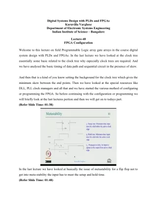
Digital Systems Design with PLDs and FPGAs Kuruvilla Varghese Department of Electronic Systems Engineering Indian Institute of Science – Bangalore Lecture-40 FPGA Configuration Welcome to this lecture on field Programmable Logic array gate arrays in the course digital system design with PLDs and FPGAs. In the last lecture we have looked at the clock tree essentially some basic related to the clock tree why especially clock trees are required. And we have analysed the basic timing of data path and sequential circuit in the presence of skew. And then that is a kind of you know setting the background for the clock tree which gives the minimum skew between the end points. Then we have looked at the special resources like DLL, PLL clock managers and all that and we have started the various method of configuring or programming the FPGA. So before continuing with the configuration or programming we will briefly look at the last lectures portion and then we will get on to todays part. (Refer Slide Time: 01:38) In the last lecture we have looked at basically the issue of metastability for a flip flop not to get into meta-stability the input has to meet the setup and hold time. (Refer Slide Time: 01:48)
And for a data path or a register to register path from that requirement we developed the inequality for the minimum clock period and we developed the condition for not violation of the hold time ok. (Refer Slide Time: 02:09) And same thing with the sequential circuit or FSM where the register to register path is between the state registers, expressions are same because if you show it explicitly you know separate the source and destination, it exactly look like this. Now what was missing in this analysis was that we assume in all these in arriving at this expressions. We assume that the clock is reaching at the source and the destination at the same time which cannot be true in a chip depending on which way the clock flows the destination could be
lagging or leading the source in terms of the clock arrival. So that should be taken into consideration when analysing these expressions. (Refer Slide Time: 03:07) And that is what we have done. (Refer Slide Time: 03:11) And we have set the two conditions or two scenarios where the clock and data flows in the same direction which is called a min path problem and where the clock and the data flows in opposite direction. (Refer Slide Time: 03:28)
And we have looked at as a case where the clock and the data in opposite direction. Then in that case the source clock is kind of leading or the destination clock is lagging. So the available time for a register to register path is reduced by amount of skew. So tclock-tskew has to accommodate tcq, tcomb and tsetup. So in a sense the clock period requirement goes up and the frequency comes down. So because of this skew the frequency of operation is coming down in the opposite problem in the main path problem where the source and destination is receiving a clock which is a delayed version of the source register as far as the skew is concerned and in this case looks like the register to register path from one clock edge to the next clock edge. We are in a better position because you have tclock+tskew is the kind of time available which need to accommodate this path delay ok. So if you analyse from one edge to the next edge things looks pretty comfortable because that is easy around budget if you would have fixed the clock period as something. (Refer Slide Time: 05:09)
Then here is relaxation on the clock period so which is good in a way but the real danger as I said is that since the clock is getting skewed maybe if this data path is fast then it can violate the hold time because the clock is moving ahead and if the tco and tcomb is min then it can violate the hold time. So that is what is shown here tco min + tcomb min should be greater than the tskew max and thold. So if it is not so it can violate and if there is a violation happens kind of reducing the clock frequency is of no use ok, because in earlier problem we sorted out suppose we have a clock period which cannot accommodate this kind of skew then we can reduce the clock period but in a min path problem it is not related to the clock period at all because we are talking about the same edge of the clock ok. So between the same edge of the clock or between the edges which are delayed same edges which are delayed by the skew, so the only way if there is a hold time violation to avoid is increase the combinational delay or logic delay. So in a sense clock when somebody is routing the clock in a chip, if there is a relative delay between the endpoints ok whenever it is that is troublesome that can reduce the clock frequency that can create hold time violation. So there need to be a mechanism to kind of route the clock tree such that the relative delays between the end points are minimal. So that like that shows you know with respect to the earlier picture we cannot route like this you knowthat as a clock tree goes it gets you know everything gets delayed because of the loading and from this to that end the delay is very high.
So we cannot have such kind of arbitrary scheme of clock routing. The ideal thing would be that from the clock pad to any end point there should be kind of equal length of the wire and equal number of buffers and this scheme does not even help even if you insert buffer here, buffer here, buffer here and all to kind of offset the delays you know offset the loading, that does not help because the buffer delays add to this skew. So you should have the buffers which are balanced. So it is ideally like you know in a simplistic way you can put a buffer then branch another buffer and another branch you know from the main route one more branch with the buffer and so on. (Refer Slide Time: 08:03) So that the extension of that is the H clock tree where from the input point. (Refer Slide Time: 08:06)
You know you go horizontally branch then vertically branch then horizontally branch wherever there is branching then you put a buffer ok. Now that does not mean that this is just one end point where a single flip flop is connected you know there could be some kind of depending on the buffer capacity there could be 20 or 25 or so many depending on the buffer. So many flip flops are there in these branches in the last branches ok. But like if you have order of magnitude increase in the number of flip flops then you branch vertically you know each one from there you can go different vertical branches and so on ok. And the idea is that say take this end point and this endpoint and if you count the number of buffers up to the end point and take the length of the wires it will be identical. So the relative delays between the edges between end points will be minimal though from the kind of the input to the output there could be you know skew quite a bit of skew which is not much of a problem if that is a problem then you can introduce a DLL which compensate for that kind of delay ok. (Refer Slide Time: 09:34)
So that is what is a DLL is used suppose you have a clock tree which is getting loaded and because of the loading if the clock is delayed and there is a skew between the input clock and output clock then the DLL can avoid that because from the output there is a feedback to the input and there will be definitely delay a skew but how it is compensated is that tclock-tskew delay is kind of further added into the tree. So that this edge will come in kind of sink with the next edge ok. So the delay locked loop you know kind of synchronize the edge by further delaying already delayed edge you know that is how it works compared to PLL. (Refer Slide Time: 10:26) The PLL essentially the scheme looks similar you know you have the input clock and the feedback clock, but what is done is that the phase is compared and the phase difference is
converted into a voltage with a low pass filter and or some equivalent scheme ok. And a voltage control oscillator you know synthesize a clock frequency which is not the kind of delayed version of this input clock frequency as in the case of DLL. But in a PLL a new clock is synthesized ok in phase with the input clock and that has certain advantage in the sense that like if there is a jitter in the input clock in a delay locked loop that will appear as a jitter at the output because delay locked loop just delays the clock but in a PLL since it is synthesized and there is a filter which filters out the minute jitters. And the clock is kind of stable okay it is a new clock, it would not have the distortion of the input clock or the jitter of the input clock. So that way PPL is better but then you know that the PLL always act you know with kind of with a range of there is a lock range and there is time to lock and things like you know at the beginning when you start up the PLL has to get into lock so it takes certain delay for the PLL to come in to lock and all that. So that is about the PLL. (Refer Slide Time: 12:12) The current FPGAs has PLL digital clock manager which is composed of DLL for de- skewing , phase shifter, frequency multiplication, division and this give phase shift like 90 degree, 180, 270 and all that. There are clock buffers, MUXs for clocking you know clock switching and that has to be glitch less you know when it has to synchronise the edges, so there will be synchronising flip flops which synchronise you know 2 clock sources to each other. And all this can be connected in the clock path or clock tree path. (Refer Slide Time: 12:50)
So that is what we have discussed and all these special resources can be instantiated from the vendor library using the core generator tool sometime synthesis tool will infer from the code. Some time you have to write the VHDL attribute along with the code to help the synthesis tool to infer what is going on and to instantiate the correct component. (Refer Slide Time: 13:18) Then the last thing we have look at was the configuration of programming of a FPGA and this the first thing while prototyping the most suitable method is through a synchronous serial port called JTAG which is used for PCB testing, chip testing and all that which is used for FPGA configuration also. So there will be a small dongle connected to PC which can program the FPGA and then there is a serial mode where the FPGA clock a serial PROM.
And get the data and programs it. And the slave serial exactly like master serials where in the slave serial FPGA expect the clock as input and the data in synchrony with the clock normally this works in conjunction with the master serial for a kind of chained programming of the FPGA. And the select map is a bite wide or kind of programming 8 or 16 bit usually when there is a microprocessor through a parallel buss FPGA can be programmed. And the configuration bit stream can be stored in the memories of the processor okay wherever it is located maybe in a flash on the board and from there along with the firmware it can be stored and at the start up the CPU can program the FPGA. (Refer Slide Time: 14:52) So this shows a serial configuration where one FPGA is a master and another FPGA is a slave which is configured by some mode pin, three mode pins are there, the current FPGA there are only 2 mode pins. And see this is in the master mode and this is in the slave mode and you can see there is a serial PROM. The clock for the serial PROM is given by the master FPGA. Also the slave FPGA get the clock from the master and the data from the serial PROM is connected to the data input of the master of FPGA and there is a data output of the master FPGA which is connected to the data input of the second slave FPGA. Now if you have a third FPGA what you can do is that the data out of this serial port can be connected to the data in of the third FPGA and so on.
And you can combine all the bit stream of all the FPGAs and store in the this particular PROM at the beginning what happens is at the power on the FPGA start programming and or if there is a program pin is there if the program pin is made low and you know if you apply a negative you know 0 pulse then it starts programming anytime. One issue is that at the beginning these FPGA has to clear their configuration memory ok. Because it could be not a power on programing, it could be a reprogramming of the FPGA while the power is on. So all the program memory configuration memory has to be cleared and depending on the FPGA type and the size it will take variable time. So the question is that how do each FPGAs knows that the other is completed the initialisation. So there is a init pin which is an open drain output which is also sampled internally so it is an I/O pin which is open drain. So and which is pulled up so it is like it is forming a wired AND ok, if everything is high this will be high if one of them is low which is pulled low ok that is the state of this kind of wired AND connection. And what happens is that suppose if the master clears the configuration memory and it has come out. Then it will drive the init output high, so but if this slave is still in the init mode it will be driving it low. Because of this pull up resistance this still be in low and that is also input to this particular FPGA and that you know sample that input and if this still it is low it waits for other FPGAs to finish. So this kind of the init which is an I/O pin which is an open drain which forms a wired AND helps the init synchronization between the masters and slaves. So ultimately everybody initializes every FPAG initialises and come out initialize initialization. And then the master FPGA you know start getting the data okay, you know it gives the clock, it enables the clock and you can see that the init pin is connected to the output enable of the PROM so even if the clock is going unless init goes high, chip output is not enabled so the data would not come. So once the init phase is over the FPGA start clocking and get the data. So first the master FPGA programmes while it is getting programmed this DOUT is made 1 ok, the 1 is going there, so the slave wait for the there is no starting pattern of the configuration since everything is one it will wait. So the master FPGA configures itself once
the configuration is over then the slave FPGAs configuration bit comes and that is bypassed to the DOUT and the slave gets programmed ok and so on. Now while the second slave programs that leave DOUT with 1 and the third slave waits so one by one the FPGA gets programmed. And this is the pin done pin which indicates that FPGAs kind of finished programming. Now again once again this is an open drain output, so which is pulled high, so it forms wired AND again. Unless all the FPGAs done pin is high this would not go high. So this is an indication to the rest of the circuitry like you will have some like maybe a CPU which is working in conjunction with FPGAs. In that case this done pin will indicate to CPU saying that FPGA has finished configuring and normal execution can kind of continue. So if there is a CPU it will sample the done pin and wait for the FPGA configuration to be over. Once it is done then it will start enabling the normal operation or if there is another external circuitry you have to make sure that the done pin enables the rest of the circuitry otherwise there will be synchronisation problem with FPGA and the rest of the circuit. Because there is another circuit which gives input to the data, input to the FPGA and if FPGA has not configured yet those data will be lost. So this done pin has to be sampled by the rest of the circuit and normally we can assume the rest of the circuit is maybe a CPU or another programmable logic based circuit whatever it is. This has to be taken care while designing. So that shows the kind of very important kind of mechanism to program the FPGA in a chain ok the multiple or this can be single it does not matter. If there is only single FPGA you can forget about this and this works and nowadays SPI or a SPI based PROMs can be used, so the FPGA offers instead of the custom serial port, SPI port and SPI can work with 1 bit data, 2 bit data and 4 bit data. In addition this PROM itself can be programmed through the JTAG port permanently. So not only that while prototyping the FPGA can be programmed through JTAG. This SPI PROM not this PROM, the SPI type PROM can be programmed through the JTAG port which often when you buy an FPGA board these options will be available you can
program normally a SPI flash will be connected in this fashion to the FPGA so that you can program the FPGA through a JTAG port. This flash through JTAG port and if you put appropriate mode pins FPGA can be configured from the flash PROM. All that is possible and that is what is written here, all what I have done is kind of elaborated. (Refer Slide Time: 23:05) And the select map scheme where you have a CPU and you have a FPGA normally you have a synchronous byte wide or two byte wide data you know program the FPGA and these are the pins you know you have the program, chips select, write, clock and data. This is the synchronous bus INIT DONE BUSY and all that okay now the issue with such a bus is that most processor bus are not sometimes synchronous okay. Like the microcontroller bus may not be synchronous, so you may have to translate the bus protocol of the process to this synchronous protocol. So that can be achieved by a CPLD coming in between to do the protocol translation of the bus and we have discussed the CPLD in the CPLD part of the lectures and we have mentioned that CPLD is good for bus protocol translation. So that is the scenario which is shown here where the CPU has some memory which could be flash where the firmware is restored. Now the FPGA configuration bit stream can be stored here, CPU can access that read it, then you know maybe byte wide 1byte is read here, then the byte is written there, again read and write such a thing can be done using this kind of
scheme and if possible the CPU can directly write if there is a synchronous port which matches the protocol. Otherwise you will have to use some kind of parallel port instead of CPLD that can be done but which can be very slow sometime when you use the parallel port in a CPU because you have to address each port you have to use the port for clocking which can be very slow sometime ok. (Refer Slide Time: 25:05) And that shows the timing like you know every clock edge the data is coming chip select and the write bar is low and anytime the FPAG is not writing the data it will indicate the busy signal in that case the data has to be kept for one more clock you know. So it is like extending the bus cycle if the peripheral is slow, I am sure that you have studied that scheme you know normally ready normally not ready kind of system. So this is a kind of normally ready system if it is kind of nothing if the FPGA does not require more time then you keep clocking the data every clock cycle. If it requires then it indicates it is not ready or it is busy, then you extend the bus cycle by adding extra delays and this is a kind of a very simple scheme which can be implemented in a CPLD. (Refer Slide Time: 26:09)
So that is what is the kind of crocks of FPGA configuration, current FPGAs are more detail I will briefly mention it, but for Virtex these are the main ways of configuring it basically the JTAG the master serials, slave serial and I mentioned about SPI port, then the select map which is byte wide which is 8 bit or 16 bit. One thing to remember is that while FPAG is getting configured all the pins will be in tri state mode. So the rest of the circuit kind of has to make sure that while it is being configured these pins the status will be tri stated and it has to be appropriately pulled up or pull down depending on the requirement of the rest of the circuit ok the rest of the circuit is sampling one of the output of the FPGA which normally in a default state you are assuming it to be 0. But while configuration rest of the circuit comes up before the FPAG configuration then assume that one of the inputs is 0 if it is tri stated, it can create problem, so it has to be pull down. And once the FPGA is configured all the flip flops are reset using an internal reset line which the FPGA vendors don’t advise you to use as a reset you know. So in your circuit you want to reset even the power on reset you should implement the separate power on reset than this internal reset signal. Though there is a way of using that reset signal within your design it is a very kind of high, kind of lot of flip flops are connected to it so it is a very heavily loaded so it may be a better idea to reset it separately which give a good drive. (Refer Slide Time: 28:17)
Also this I just briefly mentioned because there are different you know kind of extended version of that Virtex configuration is available in recent FPGA. I have taken an example of Spartan 6, it is true of Spartan 6 or kind of Virtex 6 or Virtex 7 or any of the seven series FPGAs, so your boundary scan which is a JTAG port which can configure a single device or like we have seen in the serial mode you can change the multiple devices through the JTAG. (Refer Slide Time: 28:58) You know exactly like what we have seen here even in the JTAG there is a TDI pin which take in the data TDO pin which take out the data. So the TDO pin of FPGA can be connected to the TDI pin. So it can be chained ok. So that is possible so you can in a boundary scan you can have a single device or a chain you can program multiple device. In the master serial you can have chain you know along with slave you can have a chain of devices.
Sometime what is required is that if same configuration has to be applied to all the FPGAs okay that means all the FPGAs are of the same type and it is configured by the same bit stream it can be connected in parallel and now in the serial mode if you use SPI flash the data bit can be 1 bit, 2 bit or 4 bit. There are appropriate pins and similarly for the slave serial you know normally as I said slave serial work along with master serial for the chain. And in the select MAP you have 8 bit and 16 bit configuration you can have a single device or you can have a chain of devices in select MAP, you can have slave select MAP where the clock is in here the clock is given by the FPGA but in a slave selectMAP FPGA expect the clock from outside along with the data okay. So it is little more elaborate than the Virtex, we have studied, so I just mention so that the information is current whatever I have talked about the lookup tables logic block. And all that can be extended to these kind of new devices, but this is additional so I mentioned and another issue with the earlier FPGAs were suppose you come out with the proprietary design you put the configuration bit stream in this PROM ok. Now you send that into field on a PCB or in a product what can happen is at the power on somebody can capture this data, it is very easy because the clock is coming in synchronous data is coming. So this can be easily kind of reverse engineered and you know somebody can read the bit stream and reverse engineer the complete system ok because in a FPGA the main thing is in this PROM and that is kind of there is no security on it which stream is coming as it is it can be easily read. So it is worthwhile if it can be kind of protected because mostly this will be some intellectual property of the designer or the company which is doing the design. So what is done in the current FPGAs are that this bit stream can be encrypted using the advanced encryption scheme which is called AES using a 256 bit key, now through the JTAG port this FPGA can be programmed with that key and FPGA can be told no read back that means once it is programmed this key cannot be read back, also the configuration can be read back okay. Otherwise it is possible to read back the configuration for the purpose of verification and so on. So that also can be disabled and then you deploy that in the system that means you program this PROM with a protected bit stream, then what is going on this kind of this line is an AES
encrypted bit stream and without the knowledge of the key it is very difficult to break the scheme and this can be kind of a key can be very specific to the device, that means if a company is making an industry is making a 10000 devices each 10000 will have separate keys not the same key. (Refer Slide Time: 33:33) So that way it can be very well protected so that is available in the current FPGAs. So there is an AES encryption with 256 bit key, so the bit stream is encrypted using the BitGen tool with the 256 key encryption key is programmed into FPGA through JTAG port and once it is programmed you configure it for no read back and the configuration also cannot be read back. And AES key can be permanently fused like blowing the fuse in FPGA or it can be programmed in an internal SRAM with a battery backed you know with a battery backup which is connected externally. So one can choose those options if you permanently fuse it you cannot change that AES key, so it will be permanently programmed you will be forced to use the same key for all the bit stream you program into the flash. (Refer Slide Time: 34:32)
So that way the encryption protect the design. Another option available in the recent current FPGAs are bit stream can be compressed and which is bit older than you know not that this the Spartan 6 even before the FPGA s before had this option. Because there could be a lot of resources which are not used at all not configured at all. So there is lot of kind of redundant information that not being programmed. So that information is removed and configuration bit stream size can come down, so that has two implications one is that you can store it in a lesser memory space and it can be configured very fast, the configuration will take lesser time. Otherwise for a fixed device it will take you know kind of fixed time for the device is larger it takes larger time, but even in a large device if it is not used only 50% is used it might take you know kind of less time than the full FPGA configuration. (Refer Slide Time: 35:42)
Another possibility which is available is that suppose you know this address is suppose you are programmed a configuration here and the feel like if it is programmed in a flash and flash memory and sometime the flash can get corrupted you know suppose the flash get corrupted then the whole device may not work, the flash need to be reprogrammed okay. Nowadays it is possible you know you would have seen that earlier the computers used to update through the internet. So the drivers and the software and all that, but now you can see the set top box at your home connected to a TV it can update through the cable you know through the cable the firmware get updated, the mobile phone can get updated with the firmware over the air. So same thing can happen now the configuration through the internet or wireless network can get you know can get to the device. And the device can reprogram itself so that is a possibility. So but still you know in the field if the flash is getting corrupted it will be a good idea if you have a kind of a golden bit stream or a fallback bit stream which may not be the recent one which may be very old one which is stable okay it may happen that you update the configuration over the internet and some corruption has happened. Then you can fall back on a very stable version which is there from the beginning ok so that is what is called multi boot and that is what is shown here in this particular slide. So you can have at least one main configuration and one fall back configuration and during the
configuration if the CRC error like while the configuration bit stream is read the CRC is calculated. If there is any bit corruption CRC will give error, in that case it will fall back on the golden configuration or if the sync word detection is timed out that means at the beginning there is a sync word and if that is corrupted and there will be a Watchdog timer which is waiting for it and if it does not come that times out and in that case it can fall back it can fetch the golden configuration from a particular location and that can program the FPGA. And can recover from that particular error and this scheme of multi boot is available only in the SPI based slash PROM and the BPI based slash form okay. So in both it is available it is a very good option if you have kind of if you are deploying FPGAs in the field you should think of you know the multi boot encryption and compression and all that which will improve the reliability improve the security all that part ok. (Refer Slide Time: 39:01) Now the current FPGAs in addition to the DLL, PLL block memory and all that you have the DSP slices which allows the designer to implement the DSP algorithms very efficiently and the DSP algorithm normally use fixed point computation 18 bit mantissa may be used, and you know that in one of the major operation in signal processing algorithm is multiply and accumulate. So which requires a multiplier and an adder ok, so the DSP blocks the Xilinx FPGAs DSP blocks give you this particular option you have a pre-adder that means there are 18 bit 2's
compliment pre-adder that means you can do signed addition 18 bit in the pre-adder and that added output can go to a multiplier which is an 18 by18 multiplier. So a two 18 bits can be added and that can go to multiplier. It can multiply another 18 bit which is coming from a separate port it produces a 36 bit result. Now this can be sign extended to 48 bit and it is followed with a 48 bit 2's complement adder subtractor and there are various you know it is not that everything need to used you can use this multiplier along with the post adder or you can cascade pre adder and post adder bypassing the multiplier you can take the multiplier result outside 36 bit result. So all kinds of options are available in the DSP slice which really enables one to implement the DSP like filtering algorithm, encoders, decoders and so on. All that can be implemented very efficiently in the DSP slices and many times you just use the multiplier operator then if the data size matches then it can be implemented in the DSP slices or it can be instantiated and you can use it. (Refer Slide Time: 41:16) So this is the general architecture you have four ports, all are kind of pipeline and you can see two ports are added 18+18 will give you 18 bit result which is combined with 18 bit multiplier this output can be taken out or it can be taken to another adder which is 48 bit so this is sign extended added with you know sign extension that output is available. So this helps in implementing the DSP kind of algorithms.
And this is called DSP48A1 slice in the Spartan 6 and in addition I must mention I have not put it in the slide but I should mention that the current FPGAs allows you to use the lookup table as shift register. Because look up table is normally suppose a four input look up table you have 16 flip flops inside serving as a location. So that is connected in a chain and is available as a shift register. In this case it is called SRL 16 and that can be chained to form SRL32 and even higher 64 bit shift register up to 256 bit in some kind of Spartan 6 slice and that can be in chained across so that is you know you get a shift register implementation without using the flip flops of the slice because a number of flip flops in a slice is limited and we have seen in Virtex there are only 4 and 2+ slice 4 in a CLB. (Refer Slide Time: 43:21) So if you say implement kind of 16 bit shift register then you will end up using 4 CLBs but using one lookup table, in a CLB you can implement 16 bit shift register. So that is possible to implement and one other important very important thing with respect to FPGA so I am kind of discussing all what is remaining you know one problem with the FPGA is that you have designed something in FPGA. You know you have verified you know you have done behavior solution timing solution everything but the moment you put that design in FPGA for whatever reason if something goes wrong, you cannot and if it is an internal signal you cannot kind of debug it you cannot see what is happening inside, so what is done is that the FPGA vendors give you a logic analyser circuit which is hooked to the JTAG.
Now you can instantiate this logic analyser IP along with your design and the probes of the logic analyser can be connected to the internal signal and through the JTAG port there will be a software which is available at the tool site at the PC side and through the JTAG you can capture the waveform of the internal signal and you can analyse it and like logic analyser you can trigger say it will be kind of crazy. Because suppose you have a some kind of 8 bit data line you want to monitor ok and your clock is 200 megahertz and in one second there will be kind of 200 megahertz kind of data passing over the data bus if it is clocked at frequency then to analyse that to store all that there will not be enough memory. So you can if you know that you have a kind of hint saying that what could be going wrong. But on a particular data the error happens then you can trigger on that data and capture some data around the trigger point or after the trigger point or before the trigger point. So if you have used logic analyser you would have heard saying that pre trigger, post trigger, pre trigger 50% and so on. It depends on how much you capture before the trigger how much you capture after the trigger and the analysis is always offline. It is not that on a trigger point you capture some data and you analyse offline on the PC and try to debug it. So it is a great tool to it is like once you have some complex circuits going to the FPGA to debug this logical slices have to be used and the Xilinx call it chip Scope pro and the Altera call it signal probe and it is very easy now over the years it has become a very nice tool, only thing is that it occupies because this IP this circuit occupy some kind of space within FPGA. So if you are not really floor planning the rest of the circuit it can upset the timing performance of your design some time but then if you properly design floor plan that is not very serious issue because it does not occupy much space. (Refer Slide Time: 46:36)
So that is shown in a picture here you have the FPGA board you have a FPGA what is done is that this is the kind of the blocks you instantiate like you have a ILA pro it is a logic analyser Pro which is which has probe points which can be connected to the user port and this is the one which is connecting to JTAG and on the PC side you have a software which on the trigger it captures data transfer it to the PC and you can analyse and take action, you know that is what is the signal probing does. (Refer Slide Time: 47:15) So I am just showing the Virtex pins you have the global clock pins which is dedicated which is used which is the input to the clock tree, the mode pin for selecting the mode of programming dedicated pin, cclock which is the serial clock which can be reused as a user IO program, done, init, BUSY, the parallel port all that can be used once the programming is done it can be used as a kind of this program pin is dedicated.
But this done pin is dedicated but these can be used as user IO and the all these you know these are programming pins and there is a this is a JTAG port which is dedicated, TMS is mode select, TCK is tclock, TDI is data input and TDO data output then you have the internal VCC, IO pin, VCC , the ground and so on. So normally in the FPGA this is a scenario you will have clock pins, you have some dedicated JTAG ports, dedicated mode pins and the programming pins some are dedicated most of it is kind of can be once programming is over it can be used by the user ok. (Refer Slide Time: 48:35) So there is one point I want to mention here is something called one hot encoding which is a state machine encoding which is used in FPGAs. You see this is a state machine block diagram we have a next state logic which is decoding the input and the present state and or a 2 block diagram you know enough of it but what can happen is that we will take an example to kind of to put the background for the need of one hot encoding. (Refer Slide Time: 49:15)
Suppose you assume a finite state machine with 5 inputs 18 states and 6 outputs. So when you have 18 states it means that you have you need kind of a binary encoding 5 flip flops because it is greater than 16 less than 32 Five flip flops are required and there are 5 in inputs so if you look at the next state logic and it will get 5 input and 5 state variable. So there are total 10 input to the next state logic ok. But you know that there are 5 flip flops, so there will be D4 to D0 each of that may not use all the inputs, but we assume the worst case assume that in some case all the 5 inputs are used less likely but then let us assume the worst case so and we assume that so there are 10 input for a next state logic and once again we assume the worst case in the Virtex that means we have seen that the five input function can be implemented by cascading or 6 input or 7 input can be implemented with two 4 input lookup table. But we assume again worst case for the sake of argument, so here we have 10 input next state logic so one so for 1 CLB can implement 6 input lookup table by you know two 4 input make a 5 input, two 5 input make a 6 input so on ok. Now when you have a 10 inputs lookup table that means that you need 16 CLBs because you can implement 1 CLB can implement 6 input look up table. So you need two for seven, four for eight and so on ok. So you will end up with 16 CLB I definitely have kind of exaggerated it because it is not the case at all the input, all the next state decoding will require all the external input and it is even if there are really 10 input for some kind of decoding then that may not require the lookup table which is 10 input lookup
table, one can cascade but assume the worst case it happens one can kind of come out with such a scenario. Then what happens is that this next state logic is spread in multiple CLBs and the interconnection of that makes it slow. So this clock frequency which is tco+tlogic+tsetup and we are talking about the logic delay of the next state logic and that can become very high and it can bring down the clock frequency of the state machine and we have analysed data path and we have tried to kind of be very aggressive in the kind of the timing of the data path. And suppose we have you know designed a high-performance data path but if the state machine is slow then nothing can work, so it is not a good solution you know the problem here is made by the next state logic which is very complex ok, so the question is how to kind of reduce the complexity of the next state logic. So if you look at it again you come back to the slide we have 5 inputs, 5 state variables. So the question is can we reduce the number of state variables. So we have used some kind of binary encoding which necessitated a 5 flip flops for encoding 18 states. So why not encode 18 states in 18 flip flops ok. So while decoding instead of decoding a states you know when decode a state you do not need 5 bits representing that one state you can take 1 bit presenting that state you know that is a basic idea. (Refer Slide Time: 53:24) So you have there each state is a flip flop ok. So you take this kind of state transition like Sj get 2 transition, one from the previous state Si, one condition i and Sj there is a self loop
which is condition j. So the Dj because this is nothing but Sj, Dj corresponding to this stage j is nothing but condition i and Si, but Si is just a single flip flop. So we say it is Qi or condition j which is composed of worst case 5 inputs. And Qj because this state is represented by a single flip flop Q ok, Qj, so you have the worst case 5 inputs specifying this input condition and 2 inputs for Qi and Qj, so you have 7 input next state logic which require only maybe 2 CLB which is less spread and then we have less logic delay and timing, the clock frequency becomes manageable ok. That is the idea of one hot encoding. So there is many a times people blindly like when you see a FPGA you just say ok let the state machine be one hot encoded it is not required, suppose you have four state machine with 2 input and 2 output absolutely there is no need to go for one hot encoding because this can be encoded using 2 flip flops and with 2 input the next state logic can go in one lookup table for particular flip flop. And there is absolutely no need of going for one hot encoding. So but when the number of states are more, number of inputs are more then you can go for one hot encoding which eats up the flip flop but the timing becomes better which definitely is at the cost of extra flip flops but the timing is better. So this can be kind of controlled using some kind of attribute in VHDL code you can have a state encoding like sequential which is binary like the state 0 will have 00 state 1 is kind of 1 and the grey is a grey code. And this is one-hot-one and one-hot-zero which is a single flip flop for a particular state, you know that is what is one-hot-one and one-hot-zero and this can be controlled using some attributes like saying suppose you can say suppose you have to find a state type called you know enumerated state type called type you can say attributes state encoding of state type, you can say type is grey for one-hot-one and one-hot-zero and things think like that. (Refer Slide Time: 56:27)
Or you can even specify attribute enum encoding of state type, type is you can say S0 is this i S1 i this S2 is this S3 is this you can literally specify the state encoding ok and now this is the vendor dependent this is not part of the VHDL, this is a user defined attribute, so you have to refer to the vendor tool manual whether they support it okay. So we are coming to the end of the lecture. So I will complete this part in the next lecture. Maybe another 15 minutes I will be able to complete the FPAG part then we will look at some remaining VHDL part, so today basically we have completed the configuration, we have looked at what is implemented in the current FPGA in terms of the configuration we have looked at the bit stream compression, bit stream encryption, multi boot, then we have looked at this one hot encoding where the next state logic complexity can be reduced. So that the state machine works with at a faster clock so that it is in sync with the data path and that one-hot encoding can be controlled using some attributes that is what is we have discussed today and what is remaining is very minimal we will look to complete this part. And we will look at some FPGAs from other vendors very briefly one from the Altera and one from the Actel and wind it up. Please review the portions I have covered, so that you are in sync and I wish you all the best and thank you.