Download
1 / 4
40 likes | 58 Views
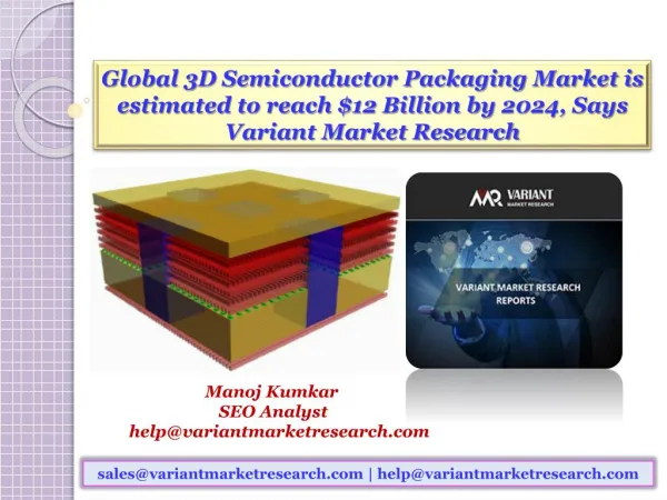
The 3D semiconductor packaging market trends paving the way for unrivaled growth in the 3D semiconductor packaging sector benefit from its distinct advantages over other packaging methods.

E N D
Benefits of 3-d Semiconductor Packaging technology The three-D semiconductor packaging market developments paving the manner for unequalled boom within the 3-d semiconductor packaging sector advantage from its distinct benefits over other packaging methods. Semiconductor Review : With the elevated usage of cellular and different electronic gadgets, expectancies for precise product performance have inevitably risen extensively. And, because of this shift, the utilization of 3D components has emerged to suit those expectations. This high-end packing approach of semiconductor chips, wherein layers of energetic digital additives get heaped collectively, enables two or greater gadgets to perform as a unmarried piece of tool. With decreased space intake, 3D semiconductor packaging technology improves performance and overall overall performance, in the long run supplanting other advanced packaging techniques.
Advantages of 3D Semiconductor Packaging Technology by way of incorporating heterogeneous semiconductor technology into microelectronic modules, three-D semiconductor permits miniaturization, which might also get utilized in beneficial microelectronics systems like diverse bio-clinical answers, sensors, and smartphones. these gadgets can also get used in big-scale computing systems like supercomputers and servers. furthermore, in terms of product utility, 3-D era is useful in a couple of way. 3D semiconductor packaging is probably a high-quality solution for increasing bandwidth, improving overall performance, and lowering fees.
Semiconductor Packaging Technology More and more complicated market needs require semiconductor fabs to search for methods to decorate manufacturing flexibility, time to marketplace, and profitability, whether or not they may be integrated device makers or fabless/foundry models. The complexities of developing, manufacturing, and bringing merchandise to market are growing, as is the fee at which new goods are delivered.organizations are tying product layout and testing to production to meet these desires, taking into account closed-loop feedback on each the product and the method. clever production in semiconductors is all about optimizing approaches from idea to design via manufacturing and servicing, no longer only linked devices inside the fab.
Read More : ● Semiconductor Review ● Key Advantages of Smart Fabs in Semiconductor Manufacturing ● Types of Advanced Packaging for Semiconductors